NTA-UGC-NET 2021 Dec & 2022 June Paper-2
May 30, 2024Number-Systems
May 31, 2024GATE 2019
|
Question 12
|
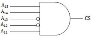
The chip select logic for a certain DRAM chip in a memory system design is shown below. Assume that the memory system has 16 address lines denoted by A15 to A0. What is the range of addresses (in hexadecimal) of the memory system that can get enabled by the chip select (CS) signal?
|
C800 to C8FF
|
|
|
C800 to CFFF
|
|
|
DA00 to DFFF
|
|
|
CA00 to CAFF
|
Question 12 Explanation:
Total address space from A0 – A15 = 215
The chip select address for given figure:
A4 – A15 = 25
So, total addressable loactions = 216/25 = 211
211 = 2048 or location 0 to 2047
∴ CFFF – C800 = 2047
Answer is C800 to CFFF.
The chip select address for given figure:
A4 – A15 = 25
So, total addressable loactions = 216/25 = 211
211 = 2048 or location 0 to 2047
∴ CFFF – C800 = 2047
Answer is C800 to CFFF.
Correct Answer: B
Question 12 Explanation:
Total address space from A0 – A15 = 215
The chip select address for given figure:
A4 – A15 = 25
So, total addressable loactions = 216/25 = 211
211 = 2048 or location 0 to 2047
∴ CFFF – C800 = 2047
Answer is C800 to CFFF.
The chip select address for given figure:
A4 – A15 = 25
So, total addressable loactions = 216/25 = 211
211 = 2048 or location 0 to 2047
∴ CFFF – C800 = 2047
Answer is C800 to CFFF.