Electronics
Question 1 |
If the channel is band limited to 6 kHz and signal to noise ratio is 16, what would be the capacity of channel?
16.15kbps | |
23.24 kbps | |
40.12 kbps | |
24.74 kbps |
Question 1 Explanation:
→ Shannon Capacity (Noisy Channel) In presence of Gaussian band-limited white noise, Shannon-Hartley theorem gives the maximum data rate capacity.
C=B log 2 (1+S/N).
where S and N are the signal and noise power, respectively, at the output of the channel.
→ This theorem gives an upper bound of the data rate which can be reliably transmitted over a thermal-noise limited channel. =6 * log 2 (1+16)
=6 * 4.08746284125034
=24.74 kbps
C=B log 2 (1+S/N).
where S and N are the signal and noise power, respectively, at the output of the channel.
→ This theorem gives an upper bound of the data rate which can be reliably transmitted over a thermal-noise limited channel. =6 * log 2 (1+16)
=6 * 4.08746284125034
=24.74 kbps
Question 2 |
At 100% modulation, the power in each sideband is__ of that of arrier.
50% | |
40% | |
60% | |
25% |
Question 2 Explanation:
→ Power in sidebands may be calculated as modulation index.
→ Each sideband is 25%. Total modulation index=1.
→ Each sideband is 25%. Total modulation index=1.
Question 3 |
The capacity relationship is given by
C=Wlog 2 (1+S/N) | |
C=2Wlog 2 (1+S/N) | |
C=Wlog 2 (1-S/N) | |
C=Wlog 10 (1+S/N) |
Question 3 Explanation:
→ Shannon Capacity (Noisy Channel) In presence of Gaussian band-limited white noise, Shannon-Hartley theorem gives the maximum data rate capacity.
C=W log 2 (1+S/N).
where S and N are the signal and noise power, respectively, at the output of the channel.
→ This theorem gives an upper bound of the data rate which can be reliably transmitted over a thermal-noise limited channel.
C=W log 2 (1+S/N).
where S and N are the signal and noise power, respectively, at the output of the channel.
→ This theorem gives an upper bound of the data rate which can be reliably transmitted over a thermal-noise limited channel.
Question 4 |
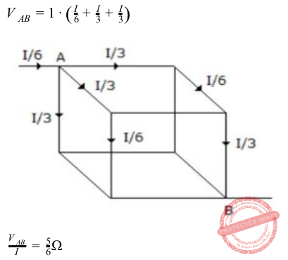
Twelve 1 Ω resistances are used as edges to form a cube. The resistance between two diagonally opposite corners of the cube is
5/6 Ω | |
1/6 Ω | |
6/5 Ω | |
3/2 Ω |
Question 4 Explanation:
Question 5 |
The final value theorem is used to find the
Steady state value of the system output | |
Initial value of the system output | |
Transient behaviour of the system output | |
None of these |
Question 5 Explanation:
The final value theorem is used to find the steady state value of the system output
Question 6 |
For the discrete signal x[n]=a n u[n], a>0 the z-transform is
(z+a)/z | |
(z-a)/z | |
z/(z-a) | |
z/(z+a) |
Question 6 Explanation:
Let x[n] be causal signal given by x[n] = a n u[n]
→ The Z-Transform of x[n] is given by
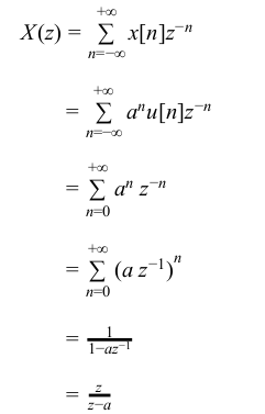
The ROC is defined by | az −1 | < 1 or | z| > | a| .
Region of Convergence(RoC)
Region of Convergence for a discrete time signal x[n] is dened as a continuous region in z plane where the Z-Transform converges. In order to determine RoC, it is convenient to represent the Z-Transform as a is rational X(z)=P(z)/Q(z)
1. The roots of the equation P(z) = 0 correspond to the ’zeros’ of X(z)
2. The roots of the equation Q(z) = 0 correspond to the ’poles’ of X(z)
3. The RoC of the Z-transform depends on the convergence of the polynomials P(z) and Q(z).
→ The Z-Transform of x[n] is given by
The ROC is defined by | az −1 | < 1 or | z| > | a| .
Region of Convergence(RoC)
Region of Convergence for a discrete time signal x[n] is dened as a continuous region in z plane where the Z-Transform converges. In order to determine RoC, it is convenient to represent the Z-Transform as a is rational X(z)=P(z)/Q(z)
1. The roots of the equation P(z) = 0 correspond to the ’zeros’ of X(z)
2. The roots of the equation Q(z) = 0 correspond to the ’poles’ of X(z)
3. The RoC of the Z-transform depends on the convergence of the polynomials P(z) and Q(z).
Question 7 |
For a periodic signal v(t)=30 sin 100t+10cos 300t +6 sin (500t + π /4), the fundamental frequency in rad/s
100 | |
300 | |
500 | |
None of the above |
Question 7 Explanation:
Given, the signal
V (t) = 3 0 sin 100t + 10 cos 300t + 6 sin (500t + π/4)
So, we have
ω 1 = 100 rads
ω 2 = 300 rads
ω 3 = 500 rads
∴ The respective time periods are
T 1 = 2π/ω1 = 2π/100 sec
T 2 = 2π/ω2 = 2π/300 sec
T 3 = 2π/ω3 = 2π/500 sec
So, the fundamental time period of the signal is
LCM (T 1 , T 2 , T 3 ) =LCM (2π,2π,2π)/HCF (100,300,500)
as T 0 =2π/100
∴ The fundamental frequency, ω0 =2π/T 0 = 100 rad/s
Question 8 |
If the number of bits per sample in a PCM system is increased from a n to n+1, the improvement in signal to quantization noise ratio will be
3dB | |
6db | |
2n dB | |
n dB |
Question 8 Explanation:
(S/N q)dB
= (1.76 + 6 n) dB
(SQNR) 1 = 1 .76 + 6 n
(SQNR) 2 = 1 .76 + 6 n(n + 1 ) = 1 .76 + 6 n + 6
(SQNR) 2 − (SQNR) 1 = 1 .76 + 6 n + 6 − 1 .76 − 6 n = 6 dB
So for every one bit increase in bits per sample will result is 6 dB improvement in signal to quantization ratio.
= (1.76 + 6 n) dB
(SQNR) 1 = 1 .76 + 6 n
(SQNR) 2 = 1 .76 + 6 n(n + 1 ) = 1 .76 + 6 n + 6
(SQNR) 2 − (SQNR) 1 = 1 .76 + 6 n + 6 − 1 .76 − 6 n = 6 dB
So for every one bit increase in bits per sample will result is 6 dB improvement in signal to quantization ratio.
Question 9 |
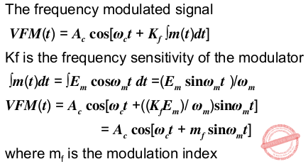
A carrier A c Cos(w C )t is frequency modulated by a signal E m Cos(w m )t. The modulation index is m f . the expression for the resulting FM signal is
A c, Cos[w c t+ m f Sin(w m )t] | |
A c Cos[w c t+ m f Cos(w m )t] | |
A c Cos[w c t+ π m f Sin w m t] | |
A c Cos[w c t+ 2 π m f E m Cos(w m )t/w m ] |
Question 9 Explanation:
Question 10 |
The open loop transfer function of a feedback control system is G(s).H(s)=1/(S+1) 3 . The gain margin of the system is
2 | |
4 | |
8 | |
16 |
Question 10 Explanation:
Given data,
The open loop transfer function of a feedback control system is G(s).H(s)=1/(S+1) 3
Gain margin=?
→ Here, the formula is -3tan -1 (W pc ) = -180 0
tan -1 (W pc ) = -180 0 /3
= -60 0
W pc =√3 rad/sec
G(s).H(s)=1/(S+1) 3
|G(s).H(s)|=X= 1/(1+W pc 2 )
=1⁄8
G(s).H(s)=1/X
= 8
The open loop transfer function of a feedback control system is G(s).H(s)=1/(S+1) 3
Gain margin=?
→ Here, the formula is -3tan -1 (W pc ) = -180 0
tan -1 (W pc ) = -180 0 /3
= -60 0
W pc =√3 rad/sec
G(s).H(s)=1/(S+1) 3
|G(s).H(s)|=X= 1/(1+W pc 2 )
=1⁄8
G(s).H(s)=1/X
= 8
Question 11 |
An ideal op-amp is an ideal
Voltage controlled current source | |
voltage controlled voltage source | |
current controlled current source | |
current controlled voltage source |
Question 11 Explanation:
An ideal op-amp lead us to an op-amp with input resistance is infinite, so no current flows into either input terminal (the “current rule”) and that the differential input offset voltage is zero (the “voltage rule”).
Ideal operational amplification will have
➝ High input impedance ( R in = ∞ ) and low output impedance ( R out = 0 )
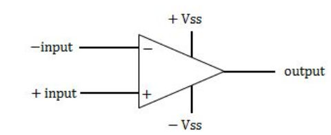
➝ R in = ∞ , so zero input current
➝ Infinite voltage gain
➝ So, it is a voltage controlled voltage source device.
Ideal operational amplification will have
➝ High input impedance ( R in = ∞ ) and low output impedance ( R out = 0 )
➝ R in = ∞ , so zero input current
➝ Infinite voltage gain
➝ So, it is a voltage controlled voltage source device.
Question 12 |
A solution for the differential equation x'(t) + 2x(t) = δ (t) with initial condition x(~0)=0
e -2t u(t) | |
e 2t u(t) | |
e -t u(t) | |
e t u(t) |
Question 13 |
In MOSFET fabrication, the channel length is delayed during the process of
Isolation oxide growth | |
Channel stop implantation | |
Ply-Silicon gate patterning | |
Lithography step leading to the contact pad |
Question 13 Explanation:
In MOSFET fabrication channel length is defined during Poly-Silicon gate patterning process
Question 14 |
The open loop transfer function of a feedback control system is G(s).H(s)=1/(S+1) 3 . The gain margin of the system is
2 | |
4 | |
8 | |
16 |
Question 14 Explanation:
The open loop transfer function of a feedback control system is G(s).H(s)=1/(S+1) 3
Gain margin=?
→ Here, the formula is -3tan -1 (W pc ) = -180 0 tan -1 (W pc ) = -180 0 /3
= -60 0
W pc =√3 rad/sec
G(s).H(s)=1/(S+1) 3
|G(s).H(s)|=X= 1/(1+W pc 2 )
=1⁄8
G(s).H(s)=1/X
= 8
Gain margin=?
→ Here, the formula is -3tan -1 (W pc ) = -180 0 tan -1 (W pc ) = -180 0 /3
= -60 0
W pc =√3 rad/sec
G(s).H(s)=1/(S+1) 3
|G(s).H(s)|=X= 1/(1+W pc 2 )
=1⁄8
G(s).H(s)=1/X
= 8
Question 15 |
The final value theorem is used to find the
Steady state value of the system output | |
Initial value of the system output | |
Transient behaviour of the system output | |
None of these |
Question 15 Explanation:
The final value theorem is used to find the steady state value of the system output
Question 16 |
For the discrete signal x[n]=a n u[n], a>0 the z-transform is
(z+a)/z | |
(z-z)/z | |
z/(z-a) | |
z/(z+a) |
Question 16 Explanation:
Let x[n] be causal signal given by x[n] = a n u[n]
→ The Z-Transform of x[n] is given by
Region of Convergence(RoC)
Region of Convergence for a discrete time signal x[n] is dened as a continuous region in z plane where the Z-Transform converges. In order to determine RoC, it is convenient to represent the Z-Transform as a is rational X(z)=P(z)/Q(z)
1. The roots of the equation P(z) = 0 correspond to the ’zeros’ of X(z)
2. The roots of the equation Q(z) = 0 correspond to the ’poles’ of X(z)
3. The RoC of the Z-transform depends on the convergence of the polynomials P(z) and Q(z).
Question 17 |
For a periodic signal v(t)=30 sin 100t+10cos 300t +6 sin (500t + π /4), the fundamental frequency in rad/s
100 | |
300 | |
500 | |
None of the above |
Question 17 Explanation:
Given, the signal
V (t) = 3 0 sin 100t + 10 cos 300t + 6 sin (500t + π/4)
So, we have
ω 1 = 100 rads
ω 2 = 300 rads
ω 3 = 500 rads
∴ The respective time periods are
T 1 = 2π/ω1 = 2π/100 sec
T 2 = 2π/ω2 = 2π/300 sec
T 3 = 2π/ω3 = 2π/500 sec
So, the fundamental time period of the signal is
LCM (T 1 , T 2 , T 3 ) =LCM (2π,2π,2π)/HCF (100,300,500)
as T 0 =2π/100
∴ The fundamental frequency, ω0 =2π/T 0 = 100 rad/s
V (t) = 3 0 sin 100t + 10 cos 300t + 6 sin (500t + π/4)
So, we have
ω 1 = 100 rads
ω 2 = 300 rads
ω 3 = 500 rads
∴ The respective time periods are
T 1 = 2π/ω1 = 2π/100 sec
T 2 = 2π/ω2 = 2π/300 sec
T 3 = 2π/ω3 = 2π/500 sec
So, the fundamental time period of the signal is
LCM (T 1 , T 2 , T 3 ) =LCM (2π,2π,2π)/HCF (100,300,500)
as T 0 =2π/100
∴ The fundamental frequency, ω0 =2π/T 0 = 100 rad/s
Question 18 |
If the number of bits per sample in a PCM system is increased from a n to n+1, the improvement in signal to quantization noise ratio will be
3 dB | |
6 db | |
2n dB | |
n dB |
Question 18 Explanation:
(S/N q)dB
= (1.76 + 6 n) dB
(SQNR) 1 = 1 .76 + 6 n
(SQNR) 2 = 1 .76 + 6 n(n + 1 ) = 1 .76 + 6 n + 6
(SQNR) 2 − (SQNR) 1 = 1 .76 + 6 n + 6 − 1 .76 − 6 n = 6 dB
So for every one bit increase in bits per sample will result is 6 dB improvement in signal to quantization ratio.
= (1.76 + 6 n) dB
(SQNR) 1 = 1 .76 + 6 n
(SQNR) 2 = 1 .76 + 6 n(n + 1 ) = 1 .76 + 6 n + 6
(SQNR) 2 − (SQNR) 1 = 1 .76 + 6 n + 6 − 1 .76 − 6 n = 6 dB
So for every one bit increase in bits per sample will result is 6 dB improvement in signal to quantization ratio.
Question 19 |
At 100% modulation, the power in each sideband is__ of that of carrier.
50% | |
40% | |
60% | |
25% |
Question 19 Explanation:
Power in sidebands may be calculated as modulation index.
→ Each sideband is 25%. Total modulation index=1.
→ Each sideband is 25%. Total modulation index=1.
Question 20 |
Twelve 1 Ω resistances are used as edges to form a cube. The resistance between two diagonally opposite corners of the cube is
5/6 Ω | |
1/6 Ω | |
6/5 Ω | |
3/2 Ω |
Question 20 Explanation:
Apply Ohms law, the resistance is equal to the voltage divided by the current. The resulting equivalent resistance is 5/6 Ω.
R=E/I
R=(2*(1/2)V)/3A
= ⅚
Note: This is the cube structure consisting of 12 resistors electrically connected between the 8 vertices. Each resistor is 1 Ω, but any value can be used so long as they are all the same.
R=E/I
R=(2*(1/2)V)/3A
= ⅚
Note: This is the cube structure consisting of 12 resistors electrically connected between the 8 vertices. Each resistor is 1 Ω, but any value can be used so long as they are all the same.
Question 21 |
A solution for the differential equation x'(t) + 2x(t) = δ (t) with initial condition x(~0)=0
e -2t u(t) | |
e 2t u(t) | |
e -t u(t) | |
e t u(t) |
Question 22 |
The noise due to random behavior of charge carriers is:
Partition noise | |
Industrial noise | |
Shot noise | |
Flicker noise |
Question 22 Explanation:
Shot noise is caused due to random behaviour of charge carriers. Shot noise is generated due to random emission of electrons from cathodes in electron tubes. In semiconductor devices, shot noise is generated due to random generation and recombination of electron-hole pairs
Question 23 |
The turn ratio of a transformer is 20:1. If a load of 40 ohm is connected across the secondary. What will be the effective resistance seen looking into the primary ?
800 ohm | |
4 k ohm | |
8 k ohm | |
16 k ohm |
Question 24 |
The electric flux and field intensity inside a conducting sphere is
Minimum | |
Maximum | |
Uniform | |
Zero |
Question 25 |
The effect of doping intrinsic semiconductor is to
Move the Fermi level away from the centre of forbidden band | |
Move the Fermi level towards the centre of forbidden band | |
Change the crystal structure of the semiconductor | |
To keep the Fermi level at the middle of the forbidden band |
Question 26 |
A 50KW, 3-phase, 400V, 60H induction motor runs at 1140 rpm. The % slip will be
1% | |
3% | |
5% | |
24% |
Question 27 |
Which of the following device can be used for controlling the speed of a dc motor ?
Thyratron | |
Thyristor | |
Transistor | |
Thermistor |
Question 28 |
The impulse response of an RL circuit is a
Rising exponential function | |
Decaying exponential function | |
Step function | |
Parabolic function |
Question 29 |
When the speed at which a conductor is moved through a magnetic field is increased, the induced voltage
Increases | |
Decreases | |
Remains constant | |
Reaches zero |
Question 30 |
AB is a vertical pole. The end A is on the level ground, C is the middle point of AB and P is a point on the level ground. The portion CB subtends an angle β at P. If AP = nAB, then
tan β = (n+1)/(2n2+1) | |
tan β = n/(2n2+1) | |
t an β = (n-1)/(2n2+1) | |
tan β = n / (n2+1) |
Question 31 |
There exist positive integers A, B and C, with no common factor greater than 1, such that, Alog 200 (5) + B log 200 (2) = C then what is the value of A + B + C ?
6 | |
7 | |
8 | |
9 |
Question 32 |
The addition of p-type impurity to intrinsic material creates allowable energy levels
slightly above conduction band | |
slightly below conduction band | |
slightly above valence band | |
slightly below valence band |
Question 33 |
Measurement of Hall coefficient enables the determination of
temperature coefficient | |
recovery time of stored carrier | |
Fermi level | |
type of conductivity and concentration of charge carriers |
Question 34 |
For input voltage of V m sin net, peak inverse voltage rating needed for diode in a half wave rectifier using capacitor filter is
V m | |
2V m | |
V m/√2 | |
V m /π | |
None of Above |
Question 35 |
A current signal is given by i (t) = 20e −50t . The initial and final value of current are
0 and 20 | |
20 and 0 | |
0 and 10 | |
20 and 10 |
Question 36 |
Common emitter configuration is preferred when main criterion is
Voltage gain | |
Current gain | |
Both voltage gain and current gain | |
Input impedance |
Question 37 |
Which of the following can be used for accurate and stable time base circuit in a digital frequency meter ?
Quartz | |
Carbon | |
Aluminium | |
Copper |
Question 38 |
An electric machine will have high efficiency when
Input / output is low | |
Reactive power is more | |
KWh consumption is low | |
Losses are low |
Question 39 |
Voltage across capacitor in RLC series circuit is maximum
At resonance | |
Just before resonance | |
Just after resonance | |
Much after resonance |
Question 40 |
Which of the following is the most economical method of starting a single phase motor
Resistant start method | |
Inductance start method | |
Capacitance start method | |
Split phase method |
Question 41 |
A 1 mA ammeter has a resistance of 100 ᘯ . It is to be converted to a 1 A ammeter. The value of shunt resistance is
0.001ᘯ | |
0.1001ᘯ | |
100000ᘯ | |
100ᘯ |
Question 42 |
When two resistance are connected in parallel, they have
Same resistances value | |
Same voltage across them | |
Same current passing through them | |
Different resistance value |
Question 43 |
Power consumed by purely inductive circuit is
VI | |
VIcosx | |
VI sinx | |
Zero |
There are 43 questions to complete.