Machine-Instructions
Question 1 |
Type-1, Type-2, Type-3 and Type-4. Type-1 category consists of four instructions, each with 3 integer register operands (3Rs).
Type-2 category consists of eight instructions, each with 2 floating point register operands (2Fs).
Type-3 category consists of fourteen instructions, each with one integer register operand and one floating point register operand (1R+1F).
Type-4 category consists of N instructions, each with a floating point register operand (1F).
The maximum value of N is ________.
32 | |
33 | |
34 | |
35 |
So, total number of instruction encodings = 216
There are 16 possible integer registers, so no. of bits required for an integer operand = 4
There are 64 possible floating point registers, so no. of bits required for a floating point operand = 6
Type-1 instructions:
There are 4 type-1 instructions and each takes 3 integer operands.
No. of encodings consumed by type-1 = 4 × 24 × 24 × 24 = 214.
Type-2 instructions:
There are 8 type-2 instructions and each takes 2 floating point operands.
No. of encodings consumed by Type-2 instructions = 8 × 26 x 26 = 215.
Type-3 instructions:
There are 14 type-3 instructions and each takes one integer operand and one floating point operand.
No. of encodings consumed by Type-3 instructions = 14 × 24 × 26 = 14336.
So, no. of encodings left for Type-4 = 216 − (214 + 215 + 14336) = 2048.
Since type-4 instructions take one floating point register, no. of different instructions of Type-4 = 2048 / 64 = 32.
Question 2 |
Consider the following data path of a simple non-pilelined CPU. The registers A, B, A1, A2, MDR, the bus and the ALU are 8-bit wide. SP and MAR are 16-bit registers. The MUX is of size 8 × (2:1) and the DEMUX is of size 8 × (1:2). Each memory operation takes 2 CPU clock cycles and uses MAR (Memory Address Register) and MDR (Memory Date Register). SP can be decremented locally.
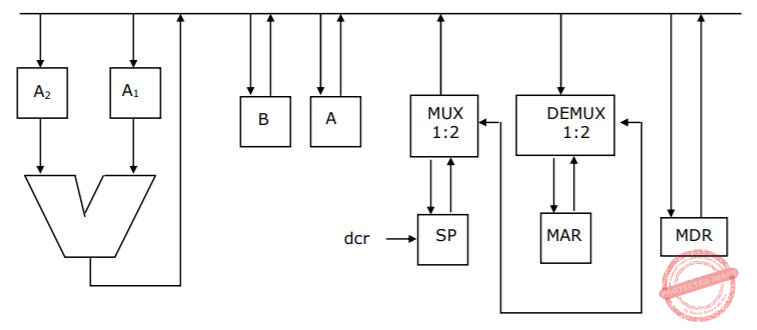
The CPU instruction “push r”, where = A or B, has the specification
     M [SP] ← r
     SP ← SP - 1
How many CPU clock cycles are needed to execute the “push r” instruction?
2 | |
3 | |
4 | |
5 |
T2: 8 → MBR, 1 cycle
T3: M[MAR] ← MBR, 2 cycles (As it is a memory operation)
So, total 5 clock cycles.
Question 3 |
Consider the following assembly language program for a hypothetical processor. A, B, and C are 8 bit registers. The meanings of various instructions are shown as comments.
     MOV B, # 0   	;   B ← 0
     MOV C, # 8	        ;   C ← 8
Z :  CMP C, # 0	        ;   compare C with 0
     JZX	        ;   jump to X if zero flag is set
     SUB C, # 1	        ;   C ← C - 1
     RRC A, # 1 	;   right rotate A through carry by one bit. Thus:
                        ;   if the initial values of A and the carry flag are a7...a0 and
                        ;   c0 respectively, their values after the execution of this
                        ;   instruction will be c0a7...a1 and a0 respectively.
     JC Y	        ;   jump to Y if carry flag is set
     JMP Z	        ;   jump to Z
Y :  ADD B, # 1	        ;   B ← B + 1
     JMP Z	        ;   jump to Z
X :
If the initial value of register A is A0 the value of register B after the program execution will be
the number of 0 bits in A0
| |
the number of 1 bits in A0 | |
A0 | |
8 |
The code is counting the number of 1 bits in A0.
Question 4 |
Consider the following assembly language program for a hypothetical processor. A, B, and C are 8 bit registers. The meanings of various instructions are shown as comments.
     MOV B, # 0   	;   B ← 0
     MOV C, # 8	        ;   C ← 8
Z :  CMP C, # 0	        ;   compare C with 0
     JZX	        ;   jump to X if zero flag is set
     SUB C, # 1	        ;   C ← C - 1
     RRC A, # 1 	;   right rotate A through carry by one bit. Thus:
                        ;   if the initial values of A and the carry flag are a7...a0 and
                        ;   c0 respectively, their values after the execution of this
                        ;   instruction will be c0a7...a1 and a0 respectively.
     JC Y	        ;   jump to Y if carry flag is set
     JMP Z	        ;   jump to Z
Y :  ADD B, # 1	        ;   B ← B + 1
     JMP Z	        ;   jump to Z
X :
Which of the following instructions when inserted at location X will ensure that the value of register A after program execution is the same as its initial value?
RRC A, #1
| |
NOP ; no operation | |
LRC A, #1 ; left rotate A through carry flag by one bit | |
ADD A, #1 |
a7, a6, a5, a4, a3 , a2, a1, a0
Now right rotate it once,
C0, a7, a6, a5, a4, a3 , a2, a1, now a0 is the new carry.
Now again right rotate it,
a0C0, a7, a6, a5, a4, a3 , a2
⁞
So after 8 rotations,
a6, a5, a4, a3 , a2, a1, a0C0 and carry is a7
Now, one more rotation will restore the original value of A0.
Hence, answer is Option (A).
Question 5 |
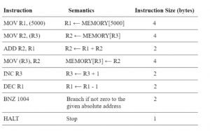
Consider the following program segment for a hypothetical CPU having three user registers R1, R2 and R3.
 Instruction 	     Operation 	      Instruction Size(in words)
 MOV R1,5000; 	 ;R1 ← Memory[5000] 	         2
 MOV R2(R1); 	 ;R2 ← Memory[(R1)] 	         1
 ADD R2,R3; 	 ;R2 ← R2 + R3 	                 1
 MOV 6000,R2; 	 ;Memory[6000] ← R2 	         2
 HALT 	         ;Machine halts 	         1
Consider that the memory is byte addressable with size 32 bits, and the program has been loaded starting from memory location 1000 (decimal). If an interrupt occurs while the CPU has been halted after executing the HALT instruction, the return address (in decimal) saved in the stack will be
1007 | |
1020 | |
1024 | |
1028 |
→ Interrupt occurs after executing halt instruction
So, number of instructions = 2+1+1+2+1 = 7
→ Each instruction with 4 bytes, then total instruction size = 7 * 4 = 28
→ Memory start location = 1000
→ Instruction saved location = 1000 + 28 = 1028
1028 is the starting address of next instruction.
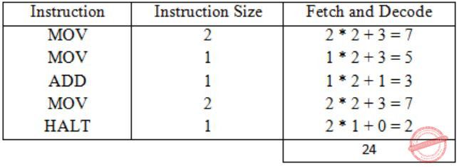
Question 6 |
Consider the following program segment for a hypothetical CPU having three user registers R1, R2 and R3.
 Instruction 	     Operation 	      Instruction Size(in words)
 MOV R1,5000; 	 ;R1 ← Memory[5000] 	         2
 MOV R2(R1); 	 ;R2 ← Memory[(R1)] 	         1
 ADD R2,R3; 	 ;R2 ← R2 + R3 	                 1
 MOV 6000,R2; 	 ;Memory[6000] ← R2 	         2
 HALT 	         ;Machine halts 	         1
Let the clock cycles required for various operations be as follows:
Register to/ from memory transfer     : 3 clock cycles
ADD with both operands in register    : 1 clock cycle
Instruction fetch and decode          : 2 clock cycles per word
The total number of clock cycles required to execute the program is
29 | |
24 | |
23 | |
20 |
Question 7 |
Assume that the content of the memory location 5000 is 10, and the content of the register R3 is 3000. The content of each of the memory locations from 3000 to 3010 is 50. The instruction sequence starts from the memory location 1000. All the numbers are in decimal format. Assume that the memory is byte addressable.
After the execution of the program, the content of memory location 3010 is _______
50 |
Register R1 will get value 10 from location 5000. So the loop in the given program will run for 10 times as the loop condition is based on ‘Dec R1’. When R1 is 0 then the loop terminates.
In these 10 iterations of the loop contents of memory locations 3000 to 3009 are changed as initial value of R3 is 3000 and in each iteration we update M[R3] ← R2 and the value of R3 is incremented to the next location 3001, 3002 etc.
But the value in location 3010 is unchanged and it will be the same as the initial value which is 50.
Question 8 |
The memory locations 1000, 1001 and 1020 have data values 18, 1 and 16 respectively before the following program is executed.
MOVI Rs, 1        ; Move immediate
LOAD Rd, 1000(Rs) ; Load from memory
ADDI Rd, 1000     ; Add immediate
STOREI 0(Rd), 20  ; Store immediate
Which of the statements below is TRUE after the program is executed?
Memory location 1000 has value 20 | |
Memory location 1020 has value 20 | |
Memory location 1021 has value 20 | |
Memory location 1001 has value 20 |
Rd ← 1
Rd ← 1001
Store in address 1001 ← 20.
Question 9 |
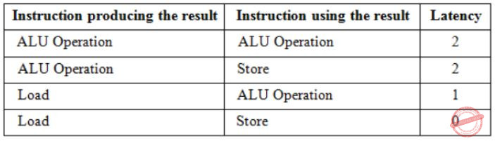
Consider the following code segment.
Load R1,Loc1;	 Load R1 from memory location Loc1
Load R2,Loc2;	 Load R2 from memory location Loc2
Add R1,R2,R1;	 Add R1 and R2 and save result in R1
Dec R2;	         Decrement R2
Dec R1;	         Decrement R1
Mpy R1,R2,R3;	 Multiply R1 and R2 and save result in R3
Store R3,Loc3;   Store R3 in memory location Loc3
What is the number of cycles needed to execute the above code segment assuming each instruction takes one cycle to execute?
7 | |
10 | |
13 | |
14 |
If an instruction is in execution phase then any other instructions cannot be in the execution phase. So, atleast 7 clock cycles will be taken.
Now, it is given that between two instructions latency or delay should be there based on their operation.
1) Load R1, Loc1;
Takes 1 clock cycle, simply loading R1 on Loc1.
2) Load R2, Loc2;
Takes 1 clock cycle.
3) Add R1, R2, R3;
Hence, this instruction is using the result of R1 and R2, i.e., result of Instruction 1 and Instruction 2. As Instruction 1 is load operation and Instruction 3 is ALU operation. So, there should be a delay of 1 clock cycle between Instruction 1 and Instruction 3, which is already there due to Instruction 2.
As Instruction 2 is load operation and Instruction 3 is ALU operation. So, there should be a delay of 1 clock cycle between Instruction 2 and Instruction 3.
4) Dec R2;
This instruction is dependent on Instruction 2 and there should be delay of one clock cycle between Instruction 2 and Instruction 4. As Instruction 2 is load and Instruction 4 is ALU, which is already there due to Instruction 2.
5) Dec R1;
This instruction is dependent on Instruction 3.
As Instruction 3 is ALU and Instruction 5 is also ALU, so a delay of 2 clock cycles should be there between them of which 1 clock cycle is already there due to Instruction 4. So, one clock delay between Instruction 4 and Instruction 5.
6) MPY R1, R2, R3;
This instruction uses the result of Instruction 5, as both Instruction 5 and Instruction 6 are ALU. So, there should be delay of 2 clock cycles.
7) Store R3, Loc3;
This instruction is dependent on Instruction 6 which is ALU and Instruction 7 is stored. So, there should be a delay of 2 clock cycles between them.
Question 10 |
Assume that EA = (X)+ is the effective address equal to the contents of location X, with X incremented by one word length after the effective address is calculated; EA = −(X) is the effective address equal to the contents of location X, with X decremented by one word length before the effective address is calculated; EA = (X)− is the effective address equal to the contents of location X, with X decremented by one word length after the effective address is calculated. The format of the instruction is (opcode, source, destination), which means (destination ← source op destination). Using X as a stack pointer, which of the following instructions can pop the top two elements from the stack, perform the addition operation and push the result back to the stack.
ADD (X)−, (X) | |
ADD (X), (X)− | |
ADD −(X), (X)+ | |
ADD −(X), (X)+ |
Lets say SP is 1000 initially then after it calculates the EA of source (which is 1000 as it decrements after the EA). The destination becomes 998 and this is where we want to store the result as stack is decrementing.
In case of C and D it becomes,
998 ← 998 + 998
Question 11 |
Consider a three word machine instruction
ADD A[R0], @B
The first operand (destination) "A[R0]" uses indexed addressing mode with R0 as the index register. The second operand (source) "@B" uses indirect addressing mode. A and B are memory addresses residing at the second and the third words, respectively. The first word of the instruction specifies the opcode, the index register designation and the source and destination addressing modes. During execution of ADD instruction, the two operands are added and stored in the destination (first operand).
The number of memory cycles needed during the execution cycle of the instruction is
3 | |
4 | |
5 | |
6 |
1 → To get 1st operand from memory address (Read).
1 → To get 2nd operand Address (Read).
1 → To get 2nd operand from the address given by previous memory (Read).
1 → To store first operand (Write).
3R + 1W = 4
Question 12 |
Consider the following data path of a CPU.
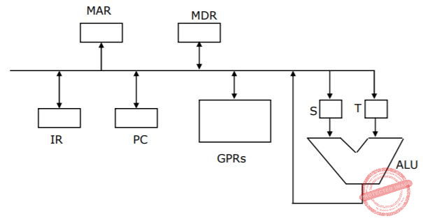
The, ALU, the bus and all the registers in the data path are of identical size. All operations including incrementation of the PC and the GPRs are to be carried out in the ALU. Two clock cycles are needed for memory read operation - the first one for loading address in the MAR and the next one for loading data from the memory bus into the MDR.
The instruction "add R0, R1" has the register transfer interpretation R0 <= R0+R1. The minimum number of clock cycles needed for execution cycle of this instruction is:
2 | |
3 | |
4 | |
5 |
1 cycle → Load PC to MAR
1 cycle → Fetch memory and load to PC
----------------------------------------------
3 cycles
----------------------------------------------
Question 13 |
Consider the following data path of a CPU.
The, ALU, the bus and all the registers in the data path are of identical size. All operations including incrementation of the PC and the GPRs are to be carried out in the ALU. Two clock cycles are needed for memory read operation - the first one for loading address in the MAR and the next one for loading data from the memory bus into the MDR.
The instruction "call Rn, sub" is a two word instruction. Assuming that PC is incremented during the fetch cycle of the first word of the instruction, its register transfer interpretation is
      Rn <= PC + 1;
      PC <= M[PC];
The minimum number of CPU clock cycles needed during the execution cycle of this instruction is:
2 | |
3 | |
4 | |
5 |
1 cycle → Load PC to MAR
1 cycle → Fetch memory and load to PC
----------------------------------------------
3 cycles
----------------------------------------------
Question 14 |
Consider a processor with byte-addressable memory. Assume that all registers, including Program Counter (PC) and Program Status Word (PSW), are of size 2 bytes. A stack in the main memory is implemented from memory location (0100)16 and it grows upward. The stack pointer (SP) points to the top element of the stack. The current value of SP is (016E)16. The CALL instruction is of two words, the first word is the op-code and the second word is the starting address of the subroutine (one word = 2 bytes). The CALL instruction is implemented as follows:
-
• Store the current value of PC in the stack.
• Store the value of PSW register in the stack.
• Load the starting address of the subroutine in PC.
The content of PC just before the fetch of a CALL instruction is (5FA0)16. After execution of the CALL instruction, the value of the stack pointer is
(016A)16 | |
(016C)16 | |
(0170)16 | |
(0172)16 |
The CALL instruction is implemented as follows:
-Store the current value of PC in the stack
pc is 2 bytes so when we store pc in stack SP is increased by 2 so current value of SP is (016E)16+2 -Store the value of PSW register in the stack
psw is 2 bytes, so when we store psw in stack SP is increased by 2
so current value of SP is (016E)16+2+2 = (0172)16