Microprocessor
Question 1 |
A single instruction to clear the lower four bits of the accumulator in 8085 assembly language?
XRI OFH | |
ANI FOH | |
XRI FOH | |
ANI OFH |
→ The XOR's don't reliably clear random bits and ANI OF clears the upper nibble, not the lower nibble.
Question 2 |
What are x and y in the following macro definition?
 macro Add x,y
 Load y
 Mul x
 Store y
 end macro
Variables | |
Identifiers | |
Actual parameters | |
Formal parameters |
Question 3 |
The following is an 8085 assembly language program:
     MVI B, OAH
     MVI A, 05H
     LXI H, IC40H
     CALL SUB
     HLT
 SUB CMP M
     RZ
     INX H
     DCR B
     JNZ SUB
     RET
(a) What does the program do?
(b) What are the contents of registers A and B initially?
(c) What are the contents of HL register pair after the execution of the program?
Theory Explanation. |
Question 4 |
A sequence of two instructions that multiplies the contents of the DE register pair by 2 and stores the result in the HL register pair (in 8085 assembly language) is:
XCHG and DAD B | |
XTHL and DAD H | |
PCHL and DAD D | |
XCHG and DAD H |
Question 5 |
Number of machine cycles required for RET instruction in 8085 microprocessor is
1 | |
2 | |
3 | |
5 |
2 for stack operation.
Total no. of cycles = 2+1 = 3
Question 6 |
An 8052 based system has an output port with address 00H. Consider the following assembly language program.
     ORG    0100H
     MVI    A, 00H
     LXI    H, 0105H
     OUT    00H
     INR    A
     PCHL
     HLT
(a) What does the program do with respect to the output port 00H?
(b) Show the wave forms at the three least significant bits of the port 00H.
Theory Explanation. |
Question 7 |
RST 7.5 interrupt in 8085 microprocessor executes the interrupt service routine from interrupt vector location
0000H | |
0075H | |
003CH | |
0034H |
→ 60 in hexa decimal is 003CH.
Question 8 |
Contents of A register after the execution of the following 8085 microprocessor program is
MVI  A, 55 H
MVI  C, 25 H
ADD  C
DAA
7AH | |
80H | |
50H | |
22H |
Question 9 |
The address space of 8086 CPU is
one Megabyte | |
256 Kilobytes | |
1 K Megabytes | |
64 Kilobytes |
Question 10 |
(a) Draw the schematic of an 8085 based system that can be used to measure the width of a pulse. Assume that the pulse is given as a TTL compatible signal by the source which generates it.
(b) Write the 8085 Assembly Language program to measure the width of the pulse. State all your assumption clearly.
Theory Explanation. |
Question 11 |
Design a 2K x 8 (2048 locations, each 8 bit wide) memory system mapped at addresses (1000)16 to (17FF)16 for the 8085 processor using four 1K x 4 memory chips. Each of these chips has the following signal pins:
- (i)
(ii)
(iii)
(iv) A0, A1, …A9(input address lines. A0 is the lest significant)
(v) D0, D1, D2, D3(bi-directional data lines. D0 is the least significant)
Theory Explanation. |
Question 12 |
To put the 8085 microprocessor in the wait state
lower the HOLD input | |
lower the READY input | |
raise the HOLD input | |
raise the READY input |
Question 13 |
The 8085 microprocessor responds to the present of an interrupt
as soon as the TRAP pin becomes ‘high’ | |
by checking the TRAP pin for ‘high’ status at the end of each instruction each | |
by checking the TRAP pin for ‘high’ status at the end of the execution of each instruction | |
by checking the TRAP pin for ‘high’ status at regular intervals |
Question 14 |
A low memory can be connected to 8085 by using
INTER | |
 | |
HOLD | |
READY |
Question 15 |
A device employing INTR line for device interrupt puts the CALL instruction on the data bus while
 | |
HOLD is active | |
READY is active | |
None of the above |
Question 16 |
In 8085 which of the following modifies the program counter?
Only PCHL instruction | |
Only ADD instructions | |
Only JMP and CALL instructions | |
All instructions |
ADD Instruction: increments the program counter.
JMP & CALL: Change the values of PC.
Question 17 |
What are the states of the Auxiliary Carry (AC) and Carry Flag (dCY) after executing the following 8085 program?
   MVI H, 5DH
   MVI L, 6BH
   MOV A, H
   ADD L
AC = 0 and CY = 0 | |
AC = 1 and CY = 1 | |
AC = 1 and CY = 0 | |
AC = 0 and CY = 1 |
⇒ H = 0101 1101
MOV L, 6BH
⇒ L = 0110 1011
MOV A, H
A = 0101 1101
ADD L ⇒ A+L =
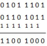
Here, AC=1; CY=0