Sequential-Circuits
Question 1 |
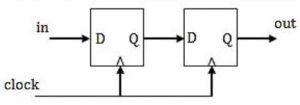
Consider the synchronous sequential circuit in the below figure.

(a) Draw a state diagram, which is implemented by the circuit. Use the following names for the states corresponding to the values of flip-flops as given below.
(b) Given that the initial state of the circuit is S4, identify the set of states, which are not reachable.
Theory Explanation. |
Question 2 |
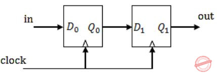
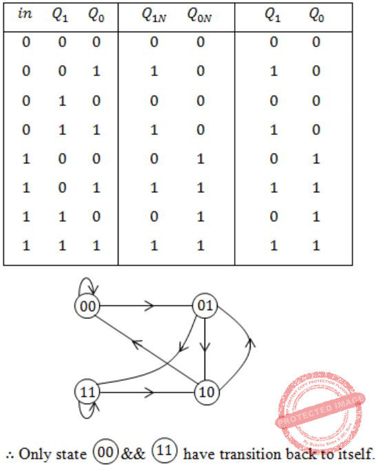
Consider the sequential circuit shown in the figure, where both flip-flops used are positive edge-triggered D flip-flops.
The number of states in the state transition diagram of this circuit that have a transition back to the same state on some value of "in" is ______
2 | |
3 | |
4 | |
5 |
Now lets draw characteristic table,
D1 = Q0
D0 = in
Question 3 |
Design a synchronous counter to go through the following states:
1, 4, 2, 3, 1, 4, 2, 3, 1, 4,...........
Theory Explanation. |
Question 4 |
The following arrangement of master-slave flip flops
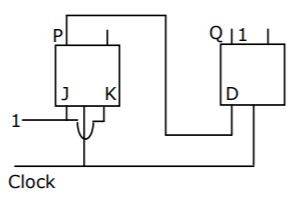
has the initial state of P, Q as 0, 1 (respectively). After three clock cycles the output state P, Q is (respectively),
1, 0 | |
1, 1 | |
0, 0 | |
0, 1 |
When 11 is applied to Jk flip flop it toggles the value of P so op at P will be 1.
Input to D flip flop will be 0(initial value of P) so op at Q will be 0.
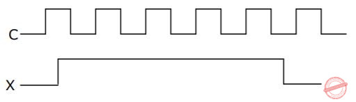
Question 5 |
Consider the following circuit with initial state Q0 = Q1 = 0. The D Flip-flops are positive edged triggered and have set up times 20 nanosecond and hold times 0.
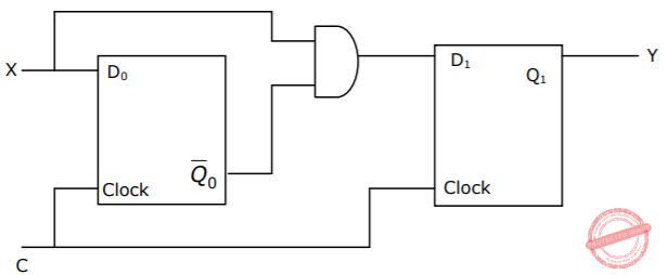
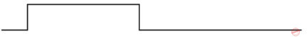
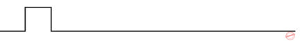
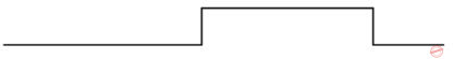
Consider the following timing diagrams of X and C; the clock period of C <= 40 nanosecond. Which one is the correct plot of Y?
 | |
 | |
 | |
 |
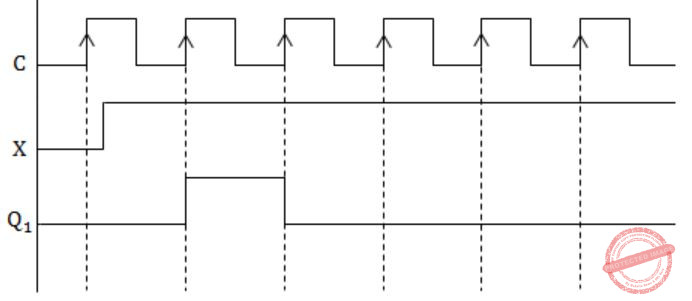
Given clock is +edge triggered.
See the first positive edge. X is 0, and hence the output is 0, because
Y = Q1N = D1×Q0' = 0⋅Q0' = 0
At second +edge, X is 1 and Q0' is also 1. So output is 1 (when second +ve edge of the clock arrives, Q0' would surely be 1 because the setup time of flip flop is given as 20ns and clock period is ≥ 40ns).
At third +ve edge, X is 1 and Q0' is 0, so output is 0.
Now output never changes back to 1 as Q0' is always 0 and when Q0' finally becomes 1, X is 0.
Hence option (A) is the correct answer.
Question 6 |
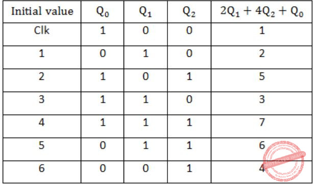
Consider the circuit given below with initial state Q0 = 1, Q1 = Q2 = 0. The state of the circuit is given by the value 4Q2 + 2Q1 + Q0
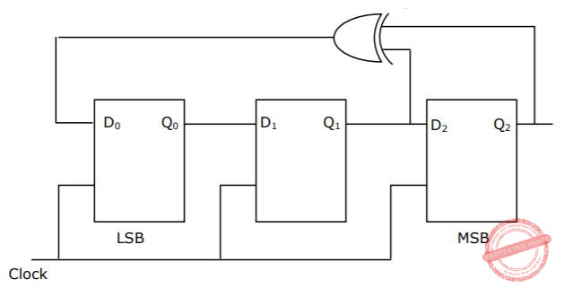
Which one of the following is the correct state sequence of the circuit?
1,3,4,6,7,5,2 | |
1,2,5,3,7,6,4 | |
1,2,7,3,5,6,4 | |
1,6,5,7,2,3,4 |
Question 7 |
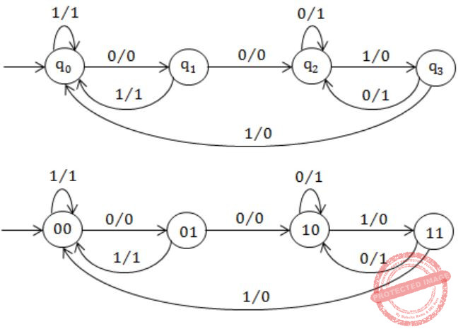
A sequential circuit takes an input stream of 0’s and 1’s and produces an output stream of 0’s and 1’s. Initially it replicates the input on its output until two consecutive 0’s are encountered on the input. From then onward, it produces an output stream, which is the bit-wise complement of input stream until it encounters two consecutive 1’s, whereupon the process repeats. An example of input and output stream is shown below.
The input stream: 101100 01001011 0 11
The desired output: 101100 10110100 0 11
J-K master-slave flip-flops are to be used to design the circuit.
(a) Give the state transition diagram.
(b) Give the minimized sum-of-product expression for J and K inputs of one of its
state flip-flops.
Theory Explanation is given below. |
Question 8 |
A 1-input, 2-output synchronous sequential circuit behaves as follows:
Let zk, nk denote the number of 0's and 1's respectively in initial k bits of the input (zk + nk = k). The circuit outputs 00 until one of the following conditions holds.
•   zk - nk = 2. In this case, the output at the k-th and all subsequent clock ticks is 10.
•   nk - zk = 2. In this case, the output at the k-th and all subsequent clock ticks is 01.
What is the minimum number of states required in the state transition graph of the above circuit?
5 | |
6 | |
7 | |
8 |
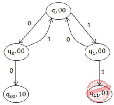
q0 ← Number of zeros is one more than number of ones.
q1 ← Number of ones is one more than number of zeros.
q00 ← Number of zeros is two more than number of ones.
q11 ← Number of ones is two more than number of zeros.
Question 9 |
In an SR latch made by cross-coupling two NAND gates, if both S and R inputs are set to 0, then it will result in
Q = 0, Q' = 1 | |
Q = 1, Q' = 0 | |
Q = 1, Q' = 1 | |
Indeterminate states |
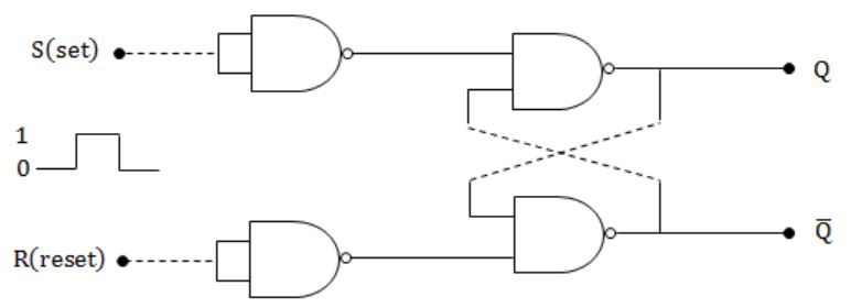
Truth table for the SR latch by cross coupling two NAND gates is
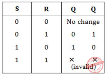
So, Answer is Option (D).
Question 10 |
Consider the partial implementation of a 2-bit counter using T flip-flops following the sequence 0-2-3-1-0, as shown below
To complete the circuit, the input X should be
Q2c | |
Q2 + Q1 | |
(Q1 + Q2)c | |
Q1 ⊕ Q2 |
0 - 2 - 3 - 1 - 0
or
00 - 10 - 11 - 01 - 00
From the given sequence, we have state table as,
Now we have present state and next state, so we should use excitation table of T flip-flop,
From state table,
T2 = Q2⊙Q1 and T1 = Q2⊕Q1
X = T1 = Q2⊕Q1
Question 11 |
Start and stop bits do not contain an ‘information’ but are used in serial communication for
Error detection | |
Error correction | |
Synchronization | |
Slowing down the communications |
Question 12 |
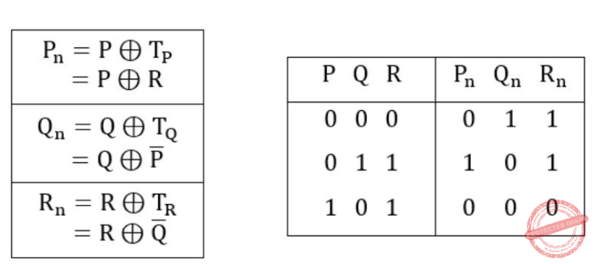
 Assuming the initial state of the counter given by PQR as 000, what are the next three states?
011, 101, 000 | |
001, 010, 111 | |
001, 010, 000 | |
011, 101, 111 |
The truth table will be
|
RQP |
Rn Qn Pn |
|
000 |
011 |
|
011 |
101 |
|
101 |
000 |
Therefore, the next three states are : 101, 000 and 011
Question 13 |
How many pulses are needed to change the contents of a 8-bit up counter from 10101100 to 00100111 (rightmost bit is the LSB)?
134 | |
133 | |
124 | |
123 |
→ First counter is move from 172 to 255 = 83 pulses
→ 255 to 0 = 1 pulse
→ 0 to 39 = 39 pulses
Total = 83 + 1 + 39 = 123 pulses
Question 14 |
Which of the following input sequences will always generate a 1 at the output Z at the end of the third cycle?
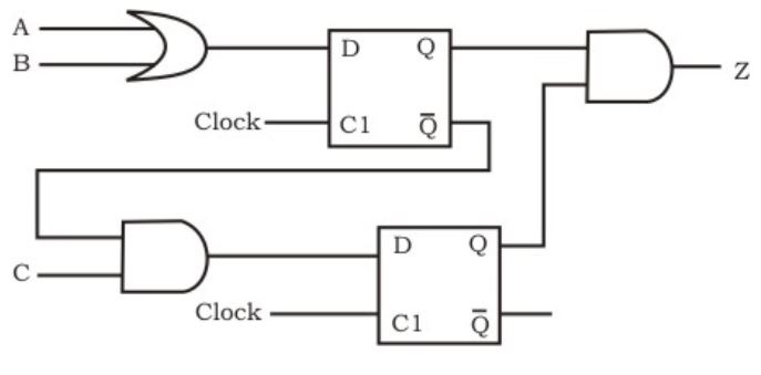
000 101 111 | |
101 110 111 | |
011 101 111 | |
001 110 111 | |
None of these |
While filling done in reverse order, all operations are not satisfied.
Question 15 |
A line L in a circuit is said to have a stuck-at-0 fault if the line permanently has a logic value 0. Similarly a line L in a circuit is said to have a stuck-at-1 fault if the line permanently has a logic value 1. A circuit is said to have a multiple stuck-at fault if one or more lines have stuck at faults. The total number of distinct multiple stuck-at faults possible in a circuit with N lines is
3N | |
3N - 1 | |
2N - 1 | |
2 |
This is because the total possible combinations (i.e., a line may either be at fault (in 2 ways i.e., stuck at 0 or 1) or it may not be, so there are only 3 possibilities for a line) is 3N. In only one combination the circuit will have all lines to be correct (i.e., not a fault). Hence, total combinations in which distinct multiple stuck-at-faults possible in a circuit with N lines is 3N - 1.
Question 16 |
The circuit shown below implements a 2-input NOR gate using two 2-4 MUX (control signal 1 selects the upper input). What are the values of signals x, y and z?
1, 0, B | |
1, 0, A | |
0, 1, B | |
0, 1, A |
g = Ax + Bz'
In MUX2, the equation is
f = xg + yg'
= x(Az+Bz') + y(Az+Bz')'
Function f should be equal to (A+B)'.
Just try to put the values of option (D), i.e., x=0, y=1, z=A,
f = 0(AA+BA') +1(AA+BA')'
= (A+B)'
∴ Option (D) is correct.
Question 17 |
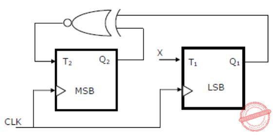
Which of the following input sequences for a cross-coupled R-S flip-flop realized with two NAND gates may lead to an oscillation?
11, 00 | |
01, 10 | |
10, 01 | |
00, 11 |
So, 00 input cause indeterminate state which may lead to oscillation.
Question 18 |
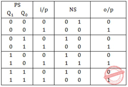
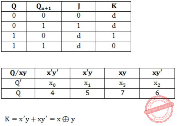
Consider the following state diagram and its realization by a JK flip flop
 The combinational circuit generates J and K in terms of x, y and Q.
The Boolean expressions for J and K are:
The combinational circuit generates J and K in terms of x, y and Q.
The Boolean expressions for J and K are:
(x⊕y)’ and x’⊕y’ | |
(x⊕y)’ and x⊕y | |
x⊕y and (x⊕y)’ | |
x⊕y and x⊕y |
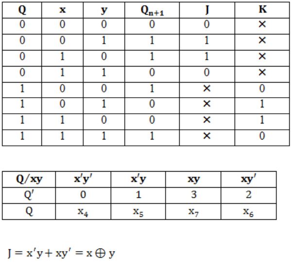
Excitation table of JK:
Question 19 |
The above circuit produces the output sequence:
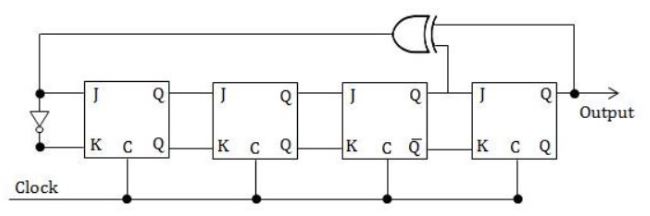
1111 1111 0000 0000 | |
1111 0000 1111 000 | |
1111 0001 0011 010 | |
1010 1010 1010 1010 |
So we can draw below table to get the output Q3.

From the above table Q3 that is output is 1111 0001 0011 010.
So, answer is (C).
Question 20 |
Choose the correct alternatives (more than one may be correct) and write the corresponding letters only: Advantage of synchronous sequential circuits over asynchronous ones is:
faster operation | |
ease of avoiding problems due to hazards | |
lower hardware requirement | |
better noise immunity
| |
none of the above
|
Question 21 |
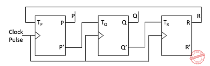
Consider the following circuit.
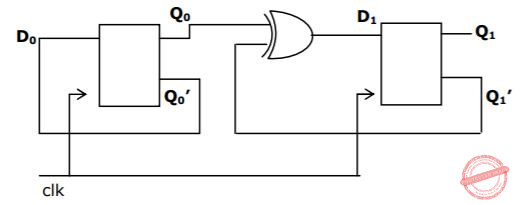
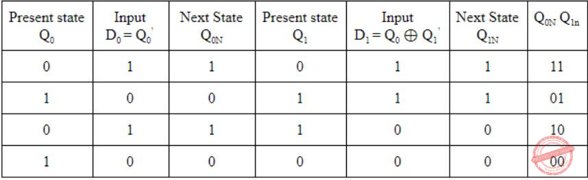
The flip-flops are positive edge triggered D FFs. Each state is designated as a two bit string Q0Q1. Let the initial state be 00. The state transition sequence is:
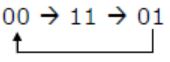 | |
 | |
 | |
 |
Question 22 |
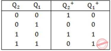
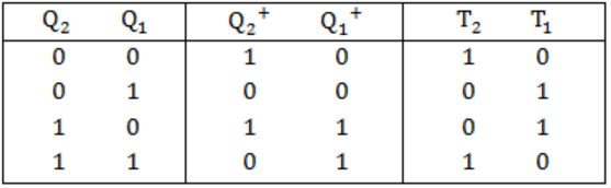
The next state table of a 2-bit saturating up-counter is given below.
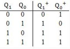
The counter is built as a synchronous sequential circuit using T flip-flops. The expressions for T1 and T0 are
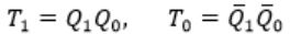 | |
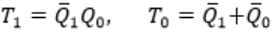 | |
 | |
 |

By using above excitation table,
Question 23 |
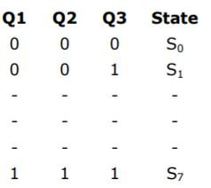
Which one of the given values of (Q1, Q2, Q3) can NEVER be obtained with this digital circuit?
(0, 0, 1) | |
(1, 0, 0) | |
(1, 0, 1) | |
(1, 1, 1) |
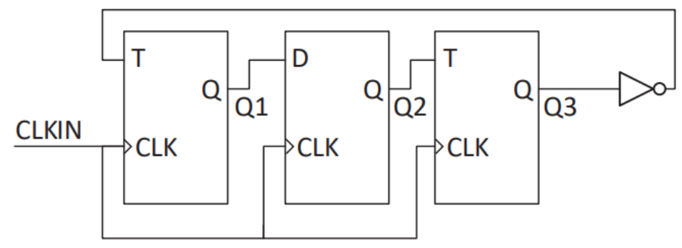
Question 24 |
The minimum number of JK flip-flops required to construct a synchronous counter with the count sequence (0, 0, 1, 1, 2, 2, 3, 3, 0, 0,……) is ___________.
2 | |
3 | |
4 | |
5 |
00
00
01
01
10
10
11
11
In the above sequence two flip-flop's will not be sufficient. Since we are confronted with repeated sequence, we may add another bit to the above sequence.
000
100
001
101
010
110
011
111
Now and every count is unique, occurring only once.
So finally 3-flip flops is required.