ISRO-2016
Question 1 |
Which of the following is true?
√3 + √7 = √10 | |
√3 + √7 ≤ √10 | |
√3 + √7 < √10 | |
√3 + √7 > √10 |
Question 1 Explanation:
√3 + √7=1.7320508075688772935274463415059 + 2.6457513110645905905016157536393
=4.3778021186334678840290620951451
√10=3.1622776601683793319988935444327
So, √3 + √7 > √10 is true.
=4.3778021186334678840290620951451
√10=3.1622776601683793319988935444327
So, √3 + √7 > √10 is true.
Question 2 |
A given connected graph is a Euler Graph if and only if all vertices of are of
same degree | |
even degree | |
odd degree | |
different degree |
Question 2 Explanation:
A given connected graph is a Euler Graph if and only if all vertices of are of even degree.
Proof:
→ Let G(V, E) be an Euler graph. Thus G contains an Euler line Z, which is a closed walk.
→ Let this walk start and end at the vertex u ∈ V. Since each visit of Z to an intermediate vertex v of Z contributes two to the degree of v and since Z traverses each edge exactly once, d(v) is even for every such vertex.
→ Each intermediate visit to u contributes two to the degree of u, and also the initial and final edges of Z contribute one each to the degree of u. So the degree d(u) of u is also even.
Question 3 |
The maximum number of edges in a n-node undirected graph without self loops is
n2 | |
n(n-1)/2 | |
n-1 | |
n(n+1)/2 |
Question 3 Explanation:
The set of vertices has size n, the number of such subsets is given by the binomial coefficient C(n,2)⋅C(n,2)=n(n-1)/2.
Question 4 |
The minimum number of NAND gates required to implement the Boolean function A + AB’+ AB’C is equal to
0 | |
1 | |
4 | |
7 |
Question 4 Explanation:
A + AB’+ AB’C = A(1+B’+B’C) = A
No GATE is required to implement the function A.
No GATE is required to implement the function A.
Question 5 |
The minimum Boolean expression for the following circuit is:
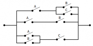
AB + AC + BC | |
A + BC | |
A + B | |
A + B + C |
Question 5 Explanation:
If the switches are in parallel then use “+”, and if they are serial then use “ ”.
A(B+C) + AB + (A+B)C = AB + AC + AB + AC + BC
= (AB+AB) + (AC+AC) + BC
= AB + AC + BC
A(B+C) + AB + (A+B)C = AB + AC + AB + AC + BC
= (AB+AB) + (AC+AC) + BC
= AB + AC + BC
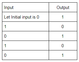
Question 6 |
For a binary half-subtractor having two inputs A and B, the correct set of logical expressions for the outputs D (= A minus B) and X (=borrow) are
D = AB + A’B , X = A’B | |
D = A’B + AB’ , X = AB’ | |
D = A’B + AB’ , X = A’B | |
D = AB + A’B , X = AB’ |
Question 6 Explanation:
The function table for the Half Subtractor is as follows
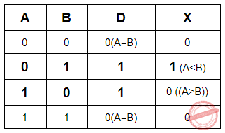 A-B= D= A’B + AB’
X= A’B
A-B= D= A’B + AB’X= A’B
Question 7 |
Consider the following gate network
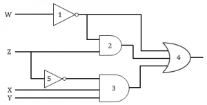
Which one of the following gates is redundant?
Which one of the following gates is redundant?
Gate No. 1 | |
Gate No. 2 | |
Gate No. 3 | |
Gate No. 4 |
Question 7 Explanation:
W’ + W’Z + Z’XY = W’(1+Z) + Z’XY
= W’ + Z’XY
The term W’Z is redundant which is represented by GATE 2.
= W’ + Z’XY
The term W’Z is redundant which is represented by GATE 2.
Question 8 |
The dynamic hazard problem occurs in
combinational circuit alone | |
sequential circuit only | |
Both (a) and (b) | |
None of the above |
Question 8 Explanation:
→ A dynamic hazard is the possibility of an output changing more than once as a result of a single input change.
→ Dynamic hazards often occur in larger logic circuits where there are different routes to the output (from the input).
→ If each route has a different delay, then it quickly becomes clear that there is the potential for changing output values that differ from the required / expected output. e.g.
→ A logic circuit is meant to change output state from 1 to 0, but instead changes from 1 to 0 then 1 and finally rests at the correct value 0. This is a dynamic hazard.
→ As a rule, dynamic hazards are more complex to resolve, but note that if all static hazards have been eliminated from a circuit, then dynamic hazards cannot occur.
Question 9 |
The logic circuit given below converts a binary code y1,y2,y3 into

Excess-3 code | |
Gray code | |
BCD code | |
Hamming Code |
Question 9 Explanation:
X1= Y1
X2= Y1⊕ Y2
X3= Y2 ⊕ Y3
X2= Y1⊕ Y2
X3= Y2 ⊕ Y3
Question 10 |
The circuit given below in the figure below is
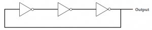
An oscillating circuit and its output is a square wave | |
The one whose output remains stable in ‘1’ state | |
The one having output remains stable in ‘0’ state | |
has a single pulse of three times propagation delay |
Question 10 Explanation:
The square wave has alternating amplitudes(0 and 1) with duty cycle 1.
An odd number of cascaded NOT gates produce a square wave.
Note: Duty cycle= Ratio of durations in which the circuit is ON and OFF in a cycle.
An odd number of cascaded NOT gates produce a square wave.
Note: Duty cycle= Ratio of durations in which the circuit is ON and OFF in a cycle.
Question 11 |
If 12A7C16 = X8, then the value of X is
224174 | |
425174 | |
6173 | |
225174 |
Question 11 Explanation:
Given, (12A7C)16 = (0001 0010 1010 0111 1100)2
MAke blocks of 3 bits each from LSB to MSB.
(Note: In the last block append zeros (as MSBs) if number bits is not three)
(000 010 010 101 001 111 100)
Each of the above blocks represents a digit in base 8 and they can be converted to base 8 as shown below.
= (0 2 2 5 1 7 4)8
MAke blocks of 3 bits each from LSB to MSB.
(Note: In the last block append zeros (as MSBs) if number bits is not three)
(000 010 010 101 001 111 100)
Each of the above blocks represents a digit in base 8 and they can be converted to base 8 as shown below.
= (0 2 2 5 1 7 4)8
Question 12 |
The Excess-3 code is also called
Cyclic Redundancy Code | |
Weighted Code | |
Self-Complementing Code | |
Algebraic Code |
Question 12 Explanation:
Excess-3 code is also called Self-Complementing Code. Because 1’s complement of an excess-3 number is equivalent to 9’s complement of the corresponding decimal digit.
→ In excess-3 code, each of the 4-bit numbers represents decimal digit which is 3 less than the actual decimal digit. So the bits have no fixed weight.
Excess-3 code is neither CRC nor Algebraic Code which is used for error detection and/or correction.
→ In excess-3 code, each of the 4-bit numbers represents decimal digit which is 3 less than the actual decimal digit. So the bits have no fixed weight.
Excess-3 code is neither CRC nor Algebraic Code which is used for error detection and/or correction.
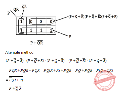
Question 13 |
The simplified SOP (Sum of Product) form the Boolean expression (P + Q’ + R’)(P + Q’ + R)(P + Q + R’)
(P’Q + R) | |
(P + Q’R’) | |
(P Q’ + R ) | |
(PQ + R) |
Question 13 Explanation:
Question 14 |
Which of the following binary number is the same as its 2’s complement?
1010 | |
0101 | |
1000 | |
1001 |
Question 14 Explanation:
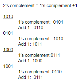 Hint: Number of bits=4
(Decimal value of maximum 4-bit number +1 )/2= (15+1)/2=8
Question 15 |
The functional difference between SR flip-flop and JK flip-flop is that
JK Flip-flop is faster than SR flip-flop | |
JK flip-flop has a feedback path | |
JK flip-flop accepts both inputs 1 | |
None of them |
Question 15 Explanation:
-> JK flip flop accepts input J=K=1. When J=K=1, the state of the flip-flop gets complimented. But it's not a valid input in SR flip-flop.
-> JK flip flop doesn’t have a feedback path.
-> JK flip flop doesn’t have a feedback path.
Question 16 |
Consider a non-pipelined processor with a clock rate of 2.5 gigahertz and average cycles per instruction of four. The same processor is upgraded to a pipelined processor with five stages; but due to the internal pipeline delay, the clock speed is reduced to 2 gigahertz. Assume that there are no stalls in the pipeline. The speedup achieved in this pipelined processor is
3.2 | |
3.0 | |
2.2 | |
2.0 |
Question 16 Explanation:
→ Given that the processor clock rate = 2.5 GHz, the processor takes 2.5 G cycles in one second.
→ Time taken to complete one cycle = (1 / 2.5 G) seconds
→ Since it is given that average number of cycles per instruction = 4, the time taken for completing one instruction=(4/2.5 G) = 1.6 ns
→ In the pipelined case we know in the ideal case CPI = 1, and the clock speed = 2 GHz.
→ Time taken for one instruction in the pipelined case = (1 / 2 G) = 0.5 ns
→ Speedup = 1.6/0.5 = 3.2
Question 17 |
What is the output of this C code?
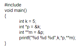
5 5 5 | |
5 5 junk | |
5 junk junk | |
Compile time error |
Question 17 Explanation:
If we are given p instead of *p then it prints the address of k but we are printing the value of k.
The same rule applies in **m.
Output is 5 5 5
The same rule applies in **m.
Output is 5 5 5
Question 18 |
Consider a disk pack with 16 surfaces, 128 tracks per surface and 256 sectors per track. 512 bytes of data are stored in a bit serial manner in a sector. The capacity of the disk pack and the number of bits required to specify a particular sector in the disk are respectively:
256 Mbyte, 19 bits | |
256 Mbyte, 21 bits | |
512 Mbyte, 20 bits | |
64 GB, 28 bits |
Question 18 Explanation:
→ Given that the disk pack has 16 surfaces, 128 tracks per surface, 256 sectors per track and each sector size is 512 bytes.
→ So the disk pack capacity = 16*128*256*512 bytes = 256 MB
→ To specify a sector we need the information about surface number, track number and sector number within a track.
→ Surface number needs 4 bits as there are 16 surfaces(24), track number needs 7 bits as there are 128 tracks(27) within a surface, within a track the sector number needs 8 bits as there are 256 sectors (28).
→ Total number bits needed to specify a particular sector = 4+7+8 = 19 bits.
Question 19 |
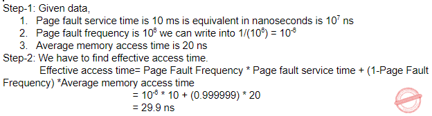
Let the page fault service time be 10 ms in a computer with average memory access time being 20 ns. If the one-page fault is generated for every 106 memory accesses, what is the effective access time for the memory?
21.4 ns | |
29.9 ns | |
23.5 ns | |
35.1 ns |
Question 19 Explanation:
Question 20 |
Register renaming is done in pipelined processors
as an alternative to register allocation at compile time | |
for efficient access to function parameters and local variables | |
to handle certain kinds of hazards | |
as part of address translation |
Question 20 Explanation:
→ Register renaming is used to eliminate hazards that arise due to WAR (Write After Read) and WAW(Write After Write) dependencies.
There are 20 questions to complete.