
digital-logic-design
Question 1 |
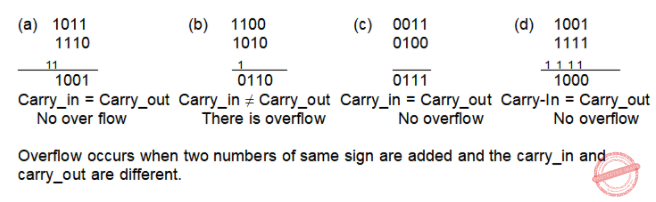
R1 = 1011 and R2 = 1110 | |
R1 = 1100 and R2 = 1010 | |
R1 = 0011 and R2 = 0100 | |
R1 = 1001 and R2 = 1111 |
Question 2 |
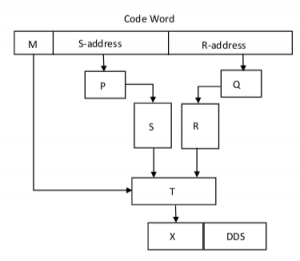
P is 10:1 multiplexer; Q is 5:1 multiplexer; T is 2:1 multiplexer | |
P is 10:2 ^10 decoder; Q is 5:2^ 5 decoder; T is 2:1 encoder | |
P is 10:2^ 10 decoder; Q is 5:2^ 5 decoder; T is 2:1 multiplexer | |
P is 1:10 de-multiplexer; Q is 1:5 de-multiplexer; T is 2:1 multiplexer |
Q is a 5:2^5 decoder that takes a 5-bit address from R-address as input and enable one of the 32 words of the R memory.
T is a 2x1 Multiplexer that select one of the 2 inputs and transmit it as output.
Question 3 |

Which one of the following is FALSE?
A + C = 0 | |
C = A + B | |
B = 3 C | |
( B - C ) > 0 |
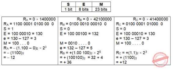
A= -12, B= +36 and C= +12
A+C= 0
B=3C
(B-C)>0
C≠A+B
Question 4 |
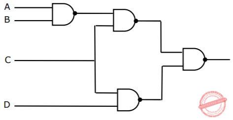
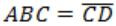
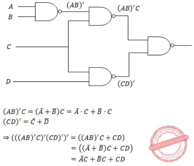
The logic expression for the output of the circuit shown in figure below is:
 | |
 | |
 | |
 | |
None of the above. |
Question 5 |
The number of flip-flops required to construct a binary modulo N counter is __________.
⌈log2 N⌉ |
Question 6 |
Consider n-bit (including sign bit) 2’s complement representation of integer number. The range of integer values, N, that can be represented is _________ ≤ N ≤ _________
-2n-1 to 2n-1 - 1 |
Question 7 |
Following 7 bit single error correcting Hamming coded message is received. (figure below):

Determine if the message is correct (assuming that at most 1 bit could be corrupted). If the message contains an error find the bit which is erroneous and gives the correct message.
Theory Explanation. |
Question 8 |
Write a program in 8085 Assembly language to Add two 16-bit unsigned BCD(8-4-2-1 Binary Coded Decimal) number. Assume the two input operands are in BC and DE Register pairs. The result should be placed in the register pair BC. (Higher order register in the register pair contains higher order digits of operand)
Theory Explanation. |
Question 9 |
Find the contents of the flip-flop Q2, Q1 and Q0 in the circuit of figure, after giving four clock pulses to the clock terminal. Assume Q2Q1Q0 = 000 initially.

Theory Explanation. |
Question 10 |
(a) Assume that a CPU has only two registers R1 and R2 and that only the following instruction is available XOR Ri, Rj; {Rj ← Ri ⊕ Rj, for i,j = 1,2}
Using this XOR instruction, find an instruction sequence in order to exchange
the contents of the registers R1 and R2.
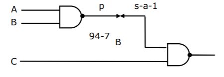
(b) The line p of the circuit shown in figure has stuck at 1 fault. Determine an input test to detect the fault.
Theory Explanation. |
Question 11 |
A multiplexer is placed between a group of 32 registers and an accumulator to regulate data movement such that at any given point in time the content of only one register will move to the accumulator. The minimum number of select lines needed for the multiplexer is _____.
5 |
A 25x1 Multiplexer with 5 select lines selects one of the 32(= 25) registers at a time depending on the selection input.
The content from the selected register will be transferred through the output line to the Accumulator.
Question 12 |
If there are m input lines and n output lines for a decoder that is used to uniquely address a byte addressable 1 KB RAM, then the minimum value of m + n is ____.
1034 |
Each output line of the decoder is connected to one of the 1K(= 1024) rows of RAM.
Each row stores 1 Byte.
m=10 and n=1024
Question 13 |
Consider the Boolean function z(a,b,c).
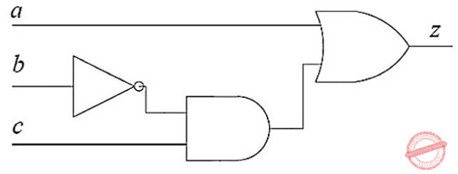
Which one of the following minterm lists represents the circuit given above?
Z = ∑(0,1,3,7) | |
Z = ∑(2,4,5,6,7) | |
Z = ∑(1,4,5,6,7) | |
Z = ∑(2,3,5) |
Convert a+b’c into canonical form which is sum of minterms.
a + b’c = a(b + b’)(c + c’) + (a + a’)b’c
= abc + abc’ + ab’c + ab’c’ + ab’c + a’b’c
= Σ(7,6,5,4,1)
Question 14 |
Consider three registers R1, R2 and R3 that store numbers in IEEE-754 single precision floating point format. Assume that R1 and R2 contain the values (in hexadecimal notation) 0x42200000 and 0xC1200000, respectively.
If R3 = R1/R2, what is the value stored in R3?
0x40800000 | |
0x83400000 | |
0xC8500000 | |
0xC0800000 |

R1 = 1.0100..0 X 2132-127
= 1.0100..0 X 25
= 101.0 X 23
= 5 X 8
= 40

R2 = (-1) x 1.0100..0 X 2130-127
= (-1) x 1.0100..0 X 23
= (-1) x 101.0 X 21
= (-1) x5 X 2
= -10
R3 = R1/R2
= -4
= (-1)x 1.0 x 22
Sign = 1
Mantissa = 000..0
Exponent = 2+127 = 129
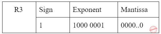
R3 = 1100 0000 1000 000..0
= 0x C 0 8 0 0 0 0 0
Question 15 |
A ROM is sued to store the table for multiplication of two 8-bit unsigned integers. The size of ROM required is
256 × 16 | |
64 K × 8 | |
4 K × 16 | |
64 K × 16 |
No. of results possible = 28 × 28 = 216 = 64K
Then total size of ROM = 64K × 16
Question 16 |
Both’s algorithm for integer multiplication gives worst performance when the multiplier pattern is
101010 …..1010 | |
100000 …..0001 | |
111111 …..1111 | |
011111 …..1110 |
Question 17 |
Consider the following floating point number representation

The exponent is in 2's complement representation and mantissa is in the sign magnitude representation. The range of the magnitude of the normalized numbers in this representation is
0 to 1 | |
0.5 to 1 | |
2-23 to 0.5 | |
0.5 to (1-2-23) |
Question 18 |
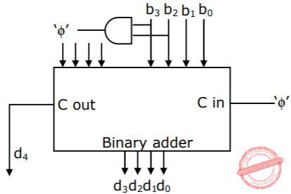
Consider the circuit given below which has a four bit binary number b3b2b1b0 as input and a five bit binary number d4d3d2d1d0 as output. The circuit implements:
Binary of Hex conversion
| |
Binary to BCD conversion | |
Binary to grey code conversion | |
Binary to radix-12 conversion |
Whenever, b2 = b3 = 1, then only 0100, i.e., 4 is added to the given binary number. Lets write all possibilities for b.
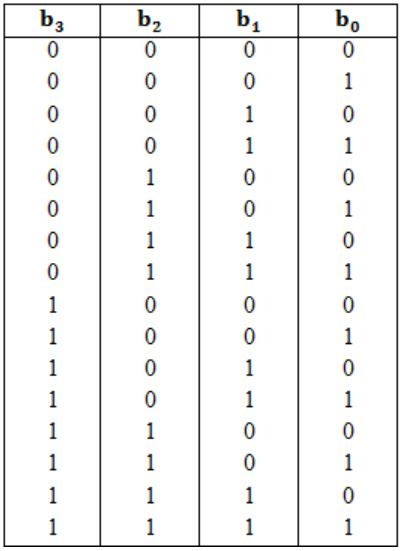
Note that the last 4 combinations leads to b3 and b2 as 1. So, in these combinations only 0010 will be added.
1100 is 12
1101 is 13
1110 is 14
1111 is 15
in binary unsigned number system.
1100 + 0100 = 10000
1101 + 0100 = 10001, and so on.
This is conversion to radix 12.
Question 19 |
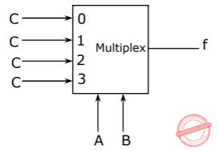
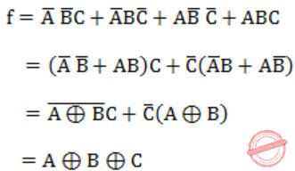
Consider the circuit in below figure. f implements
 | |
A + B + C | |
A ⊕ B ⊕ C | |
AB + BC + CA |
Question 20 |
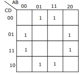
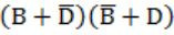
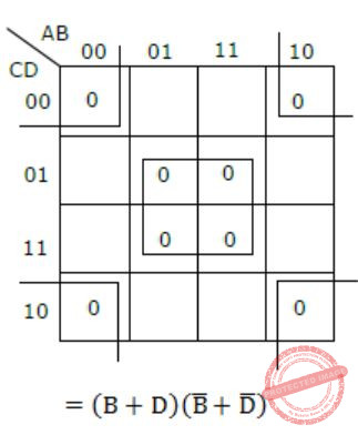
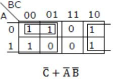
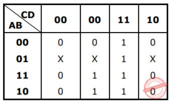
What is the equivalent Boolean expression in product-of-sums form for the Karnaugh map given below.
 | |
 | |
 | |
 | |
None of the above |

Question 21 |
A logic network has two data inputs A and B, and two control inputs C0 and C1. It implements the function F according to the following table.
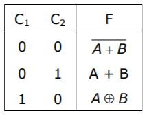
Implement the circuit using one 4 to 1 Multiplexer, one 2-input Exclusive OR gate, one 2-input AND gate, one 2-input OR gate and one Inverter.
Theory Explanation. |
Question 22 |
Consider the synchronous sequential circuit in the below figure.

(a) Draw a state diagram, which is implemented by the circuit. Use the following names for the states corresponding to the values of flip-flops as given below.
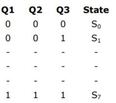
(b) Given that the initial state of the circuit is S4, identify the set of states, which are not reachable.
Theory Explanation. |
Question 23 |
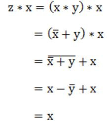
Let * be defined as x * y = x' + y. Let z = x * y. Value of z * x is
x'+y | |
x | |
0 | |
1 |
Question 24 |
An N-bit carry look ahead adder, where N is a multiple of 4, employs ICs 74181 (4 bit ALU) and 74182 (4 bit carry look ahead generator).
The minimum addition time using the best architecture for this adder is
proportional to N | |
proportional to log N | |
a constant | |
None of the above |
Question 25 |
Let f(x, y, z) = x' + y'x + xz be a switching function. Which one of the following is valid?
 | |
xz is a minterm of f | |
xz is an implicant of f | |
y is a prime implicant of f |
Question 26 |
Given √224)r = 13)r.
The value of the radix r is:
10 | |
8 | |
5 | |
6 |
Convert r base to decimal.
√2r2 + 25 + 4 = r + 3
Take square both sides,
2r2 + 2r + 4 = r2 + 6r + 9
r2 - 4r - 5 = 0
r2 - 5r + r - 5 = 0
r(r - 5) + (r - 5) = 0
r = -1, 5
r cannot be -1,
So r = 5 is correct answer.
Question 27 |
Consider a logic circuit shown in figure below. The functions f1, f2 and f (in canonical sum of products form in decimal notation) are:
f1(w,x,y,z) = ∑8,9,10
f2(w,x,y,z) = ∑7,8,12,13,14,15
f(w,x,y,z) = ∑8,9
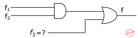
The function f3 is
Σ9,10 | |
Σ9 | |
Σ1,8,9 | |
Σ8,10,15 |
Since, f1 and f2 are in canonical sum of products form, f1⋅f2 will only contain their common terms that is f1⋅f2 = Σ8.
Now,
Σ8 + f3 = Σ8,9
So, f3= Σ9
Question 28 |
The n-bit fixed-point representation of an unsigned real number X uses f bits for the fraction part. Let i = n-f. The range of decimal values for X in this representation is
2-f to 2i | |
2-f to (2i - 2-f) | |
0 to 2i | |
0 to (2i - 2-f ) |
Number of bits in fraction part → f-bits
Number of bits in integer part → (n – f) bits
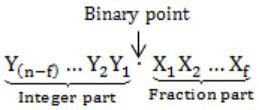
Minimum value:
000…0.000…0 = 0
Maximum value:
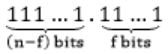
= (2 n-f - 1) + (1 - 2 -f
= (2n-f - 2 -f)
= (2i - 2 -f )
Question 29 |
When two 8-bit numbers A7...A0 and B7...B0 in 2’s complement representation (with A0 and B0 as the least significant bits) are added using a ripple-carry adder, the sum bits obtained are S7...S0 and the carry bits are C7...C0. An overflow is said to have occurred if
the carry bit C7 is 1 | |
all the carry bits (C7,…,C0) are 1 | |
 | |
 |
i.e., A7 = B7
⇾ Overflow can be detected by checking carry into the sign bits (Cin) and carry out of the sign bits (Cout).
⇾ Overflow occurs iff A7 = B7 and Cin ≠ Cout
These conditions are equivalent to

Consider
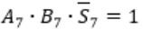
Here A7 = B7 = 1 and S7 = 0
This happens only if Cin = 0
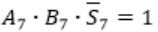
Carry out Cout=1 when
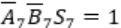
Similarly, in case of
Cin=1 and Cout will be 0.
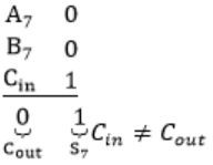
Question 30 |
Consider the Karnaugh map given below, where X represents “don’t care” and blank represents 0.
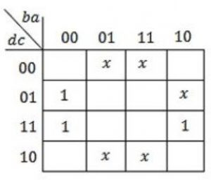
Assume for all inputs 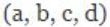 , the respective complements
 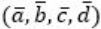 are also available. The above logic is implemented using 2-input NOR gates only. The minimum number of gates required is _________.
1 | |
2 | |
3 | |
4 |
As all variables and their complements are available we can implement the function with only one NOR Gate.
Question 31 |
Consider a combination of T and D flip-flops connected as shown below. The output of the D flip-flop is connected to the input of the T flip-flop and the output of the T flip-flop is connected to the input of the D flip-flop.
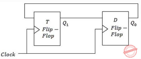
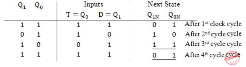
Initially, both Q0 and Q1 are set to 1 (before the 1st clock cycle). The outputs
Q1Q0 after the 3rd cycle are 11 and after the 4th cycle are 00 respectively | |
Q1Q0 after the 3rd cycle are 11 and after the 4th cycle are 01 respectively | |
Q1Q0 after the 3rd cycle are 00 and after the 4th cycle are 11 respectively | |
Q1Q0 after the 3rd cycle are 01 and after the 4th cycle are 01 respectively |

Question 32 |
What happens when a bit-string is XORed with itself n-times as shown:
[B⊕(B⊕(B⊕(B........ n times)]
complements when n is even | |
complements when n is odd | |
divides by 2n always | |
remains unchanged when n is even |
Consider:
B⊕(B⊕B)
= B⊕0
= 0 (if consider n times it remains unchanged)
Question 33 |
A multiplexor with a 4 bit data select input is a
4:1 multiplexor | |
2:1 multiplexor | |
16:1 multiplexor | |
8:1 multiplexor |
For 4 bit data it selects 24 : 1 = 16: 1 input
Question 34 |
The threshold level for logic 1 in the TTL family is
any voltage above 2.5 V | |
any voltage between 0.8 V and 5.0 V | |
any voltage below 5.0 V | |
any voltage below Vcc but above 2.8 V |
Question 35 |
The octal representation of an integer is (342)8. If this were to be treated as an eight-bit integer is an 8085 based computer, its decimal equivalent is
226 | |
-98 | |
76 | |
-30 |
If this can be treated as 8 bit integer, then the first becomes sign bit i.e., '1' then the number is negative.
8085 uses 2's complement then
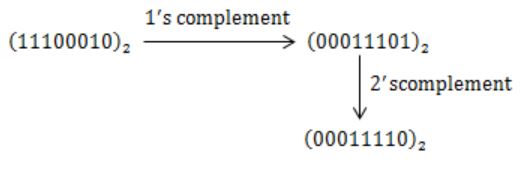
⇒ -30
Question 36 |
The function represented by the Karnaugh map given below is:
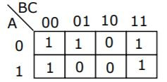
A⋅B | |
AB+BC+CA | |
 | |
None of the above |
Question 37 |
Which of the following operations is commutative but not associative?
AND | |
OR | |
NAND | |
EXOR |
Question 38 |
Suppose the domain set of an attribute consists of signed four digit numbers. What is the percentage of reduction in storage space of this attribute if it is stored as an integer rather than in character form?
80% | |
20% | |
60% | |
40% |
We have four digits. So to represent signed 4 digit numbers we need 5 bytes, 4 bytes for four digits and 1 for the sign.
So required memory = 5 bytes.
Now, if we use integer, the largest no. needed to represent is 9999 and this requires 2 bytes of memory for signed representation.
9999 in binary requires 14 bits. So, 2 bits remaining and 1 we can use for sign bit.
So, memory savings,
= 5 - 2/5 × 100
= 60%
Question 39 |
(a) The implication gate shown below, has two inputs (x and y), the output is 1 except when x=1 and y=0. Realize f = x'y + xy' using only four implication gates.
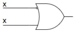
(b) Show that the implication gate is functionally complete.
Theory Explanation. |
Question 40 |
Design a synchronous counter to go through the following states:
1, 4, 2, 3, 1, 4, 2, 3, 1, 4,...........
Theory Explanation. |
Question 41 |
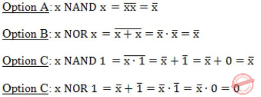
 ?
?x NAND X | |
x NOR x | |
x NAND 1 | |
x NOR 1 |
Question 42 |
 | |
 | |
 | |
 |
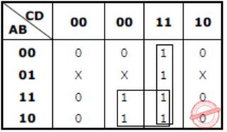
⇒ CD+AD = D(A+C)
Question 43 |
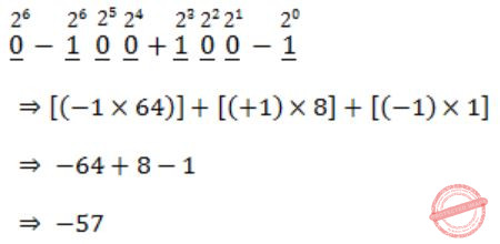
Booth’s coding in 8 bits for the decimal number –57 is
0 – 100 + 1000 | |
0 – 100 + 100 - 1 | |
0 – 1 + 100 – 10 + 1 | |
00 – 10 + 100 - 1 |
Question 44 |
The maximum gate delay for any output to appear in an array multiplier for multiplying two n bit number is
On2 | |
O(n) | |
O(log n) | |
O(1) |
Total delay = 1 * 2n - 1 = O(2n - 1) = n
Question 45 |
The number of full and half-adders required to add 16-bit numbers is
8 half-adders, 8 full-adders | |
1 half-adder, 15 full-adders | |
16 half-adders, 0 full-adders | |
4 half-adders, 12 full-adders |
But for rest of bits we need full address since carry from previous addition has to be included into the addition operation.
So, in total 1 half adder and 15 full adders are required.
Question 46 |
Zero has two representations in
Sign magnitude | |
1’s complement | |
2’s complement | |
None of the above | |
Both A and B |
+0 = 0000
-0 = 1000
1's complement:
+0 = 0000
-0 = 1111
Question 47 |
The number 43 in 2’s complement representation is
01010101 | |
11010101 | |
00101011 | |
10101011 |
Question 48 |
The simultaneous equations on the Boolean variables x, y, z and w,
x + y + z = 1
xy = 0
xz + w = 1
xy +  = 0
= 0
have the following solution for x, y, z and w, respectively.
0 1 0 0 | |
1 1 0 1 | |
1 0 1 1 | |
1 0 0 0 |
Question 49 |
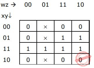
Which function does NOT implement the Karnaugh map given below?
(w + x)y | |
xy + yw | |
 | |
None of the above |
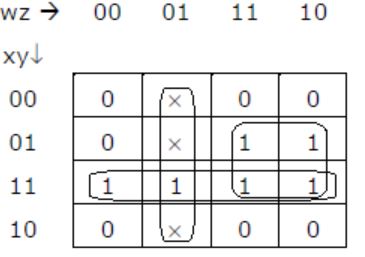
⇒ wy + wz + xy
Question 50 |
The following arrangement of master-slave flip flops
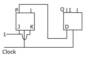
has the initial state of P, Q as 0, 1 (respectively). After three clock cycles the output state P, Q is (respectively),
1, 0 | |
1, 1 | |
0, 0 | |
0, 1 |
When 11 is applied to Jk flip flop it toggles the value of P so op at P will be 1.
Input to D flip flop will be 0(initial value of P) so op at Q will be 0.