Computer-Organization
Question 1 |
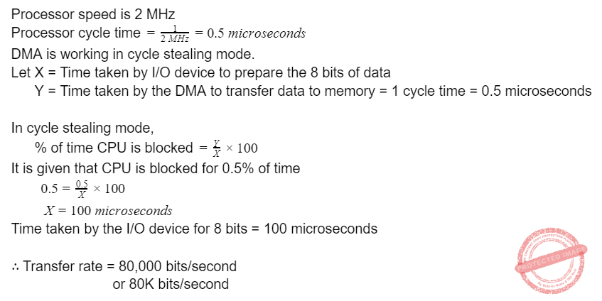
2 |
Cache size = 2KB
Block size = 64 Bytes = 2^6 bytes. So the OFFSET is 6 bits long.
The TAG field is 22 bits. And the physical address is 32 bits.
Since it is given as a set associative cache, the physical address is divided as (TAG, SET, OFFSET).
From the given information we can find the SET number = 32 - 22 - 6 = 4 bits.
Using the 4 SET bits, the number of sets possible = 2^4 = 16.
Number of blocks in the cache = Cache size / Block size = 2KB / 64 = 2^11/2^6 = 2^5.
Number of sets in the cache = Number of blocks in the cache / Number of blocks in each set
Number of blocks in each set is also called the associativity.
16 = 2^5/associativity
Associativity = 2^5/16 = 2
Question 2 |
80,000
|
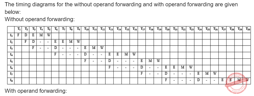
Question 3 |
Consider the following sequence of 8 instructions:
ADD, MUL, ADD, MUL, ADD, MUL, ADD, MUL
Assume that every MUL instruction is data-dependent on the ADD instruction just before it and every ADD instruction (except the first ADD) is data- dependent on the MUL instruction just before it. The Speedup is defined as follows:
Assume that every MUL instruction is data-dependent on the ADD instruction just before it and every ADD instruction (except the first ADD) is data-dependent on the MUL instruction just before it. The Speedup is defined as follows:
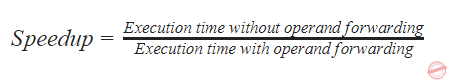
The Speedup achieved in executing the given instruction sequence on the pipelined processor (rounded to 2 decimal places) is ________.
1.875 |
Question 4 |
S1:Read misses in a write through L1 cache do not result in writebacks of dirty lines to the L2.
S2:Write allocate policy must be used in conjunction with write through caches and no-write allocate policy is used with write back caches.
S1is true and S2is false | |
S1is false and S2is false | |
S1is true and S2is true | |
S1is false and S2is true |
S1: In a write through cache the writing happens to both the L1 and L2 caches simultaneously. It is also given as the inclusive hierarchy. Here L1 is a subset of L2. So when there is a cache read miss in L1 we try to fetch the content from L2. If the block containing that missed word is dirty in the L1 cache, since it is a write through cache the same content would have also been written to the L2 cache also earlier itself. So there is no need to write back the dirty lines again to the L2 cache on a cache miss. Hence S1 is true.
S2: Generally no-write allocate is used with write through cache and write allocate is used with write back cache. Hence S2 is false.
Question 5 |
A single instruction to clear the lower four bits of the accumulator in 8085 assembly language?
XRI OFH | |
ANI FOH | |
XRI FOH | |
ANI OFH |
→ The XOR's don't reliably clear random bits and ANI OF clears the upper nibble, not the lower nibble.
Question 6 |
In a vectored interrupt
the branch address is assigned to a fixed location in memory | |
the interrupt source supplies the branch information to the processor through an interrupt vector | |
the branch address is obtained from a register in the processor | |
none of the above |
Question 7 |
The principle of locality justifies the use of
interrupts | |
DMA | |
Polling | |
Cache Memory |
→ The things which are used more frequently those are stored in locality of reference.
→ For this purpose we use the cache memory.
Question 8 |
What are x and y in the following macro definition?
 macro Add x,y
 Load y
 Mul x
 Store y
 end macro
Variables | |
Identifiers | |
Actual parameters | |
Formal parameters |
Question 9 |
The capacity of a memory unit is defined by the number of words multiplied by the number of bits/word. How many separate address and data lines are needed for a memory of 4K × 16?
10 address, 16 data lines | |
11 address, 8 data lines | |
12 address, 16 data lines | |
12 address, 12 data lines |
m = no. of address lines
n = no. of data lines
Given, 4K × 16 = 212 × 16
Address lines = 12
Data lines = 16
Question 10 |
A computer system has a 4K word cache organized in block-set-associative manner with 4 blocks per set, 64 words per block. The number of its in the SET and WORD fields of the main memory address format is:
15, 40 | |
6, 4 | |
7, 2 | |
4, 6 |
So we need 4 set bits.
And,
64 words per block means WORD bit is 6-bits.
So, answer is option (D).
Question 11 |
If the overhead for formatting a disk is 96 bytes for 4000 byte sector,
(a) Compute the unformatted capacity of the disk for the following parameters:
 Number of surfaces: 8
 Outer diameter of the disk: 12 cm
 Inner diameter of the disk: 4 cm
 Inter track space: 0.1 mm
 Number of sectors per track: 20
(b) if the disk in (a) is rotating at 360 rpm, determine the effective data transfer rate which is defined as the number of bytes transferred per second between disk and memory.
Theory Explanation. |
Question 12 |
The following is an 8085 assembly language program:
     MVI B, OAH
     MVI A, 05H
     LXI H, IC40H
     CALL SUB
     HLT
 SUB CMP M
     RZ
     INX H
     DCR B
     JNZ SUB
     RET
(a) What does the program do?
(b) What are the contents of registers A and B initially?
(c) What are the contents of HL register pair after the execution of the program?
Theory Explanation. |
Question 13 |
A sequence of two instructions that multiplies the contents of the DE register pair by 2 and stores the result in the HL register pair (in 8085 assembly language) is:
XCHG and DAD B | |
XTHL and DAD H | |
PCHL and DAD D | |
XCHG and DAD H |
Question 14 |
Consider the following statements.
- I. Daisy chaining is used to assign priorities in attending interrupts.
II. When a device raises a vectored interrupt, the CPU does polling to identify the source of the interrupt.
III. In polling, the CPU periodically checks the status bits to know if any device needs its attention.
IV. During DMA, both the CPU and DMA controller can be bus masters at the same time.
Which of the above statements is/are TRUE?
I and IV only | |
I and II only
| |
III only | |
I and III only
|
Statement-II is false as vectored interrupt doesn’t involve polling but non-vectored interrupt involves polling.
Statement-III is true as polling means that CPU periodically checks the status bits to know if any device needs attention.
Statement-IV is false as during DMA only one of the CPU or DMA can be bus master at a time.
Question 15 |
A direct mapped cache memory of 1 MB has a block ize of 256 bytes. The cache has an access time of 3 ns and a hit rate of 94%. During a cache miss, it takes 20 ns to bring the first word of a block from the main memory, while each subsequent word takes 5 ns. The word size is 64 bits. The average memory access time in ns (round off to 1 decimal place) is _____.
13.5 |
Hit ratio of cache = 0.94
Word size is 64 bits = 8 bytes.
Cache line size = 256 bytes = 32 words
Main memory access time = 20ns(time for first word) + 155ns(time for remaining 31 words, 31*5 = 155ns) = 175 ns
Average access time = h1*t1 + (1-h1)(t1+t2) = t1 +(1-h1)t2
⇒ 3 + (0.06)(175) = 13.5 ns
Question 16 |
Consider the following data path diagram.
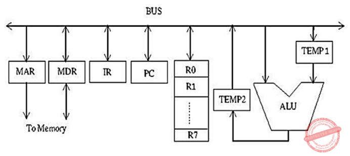
Consider an instruction: R0 ← R1 + R2. The following steps are used to execute it over the given data path. Assume that PC is incremented appropriately. The subscripts r and w indicate read and write operations, respectively.
1. R2r, TEMP1r, ALUadd, TEMP2w
2. R1r, TEMP1w
3. PCr, MARw, MEMr
4. TEMP2r, ROw
5. MDRr, IRw
Which one of the following is the correct order of execution of the above steps?
3, 5, 1, 2, 4
| |
3, 5, 2, 1, 4
| |
1, 2, 4, 3, 5 | |
2, 1, 4, 5, 3
|
First the PC value has to be moved into MAR (step-3 from the given sequence), then the instruction has to be fetched(step-5 from the given sequence). Then Temp1 is loaded with the value of R1 (step-2 from the given sequence), then the addition operation is performed by accessing the R2 value directly and adding it to Temp1 value and storing the result in Temp2 (step-1 from the given sequence).
Finally the result from Temp2 is stored in R0 (step-4 from the given sequence).
Hence the correct sequence is (3, 5, 2, 1, 4).
Question 17 |
Consider a non-pipelined processor operating at 2.5 GHz. It takes 5 clock cycles to complete an instruction. You are going to make a 5-stage pipeline out of this processor. Overheads associated with pipelining force you to operate the pipelined processor at 2 GHz. In a given program, assume that 30% are memory instructions, 60% are ALU instructions and the rest are branch instructions. 5% of the memory instructions cause stalls of 50 clock cycles each due to cache misses and 50% of the branch instructions cause stalls of 2 cycles each. Assume that there are no stalls associated with the execution of ALU instructions. For this program, the speedup achieved by the pipelined processor over the non-pipelined processor (round off to 2 decimal places) is _____.
2.16 |
It is given that each instruction takes 5 clock cycles to execute in the non-pipelined architecture, so time taken to execute each instruction = 5 * 0.4 = 2ns
In the pipelined architecture the clock cycle time = 1/2G = 0.5 ns
In the pipelined architecture there are stalls due to memory instructions and branch instructions.
In the pipeline, the updated clocks per instruction CPI = (1 + stall frequency due to memory operations * stalls of memory instructions + stall frequency due to branch operations * stalls due to branch instructions)
Out of the total instructions , 30% are memory instructions. Out of those 30%, only 5% cause stalls of 50 cycles each.
Stalls per instruction due to memory operations = 0.3*0.05*50 = 0.75
Out of the total instructions 10% are branch instructions. Out of those 10% of instructions 50% of them cause stalls of 2 cycles each.
Stalls per instruction due to branch operations = 0.1*0.5*2 = 0.1
The updated CPI in pipeline = 1 + 0.75 + 0.1 = 1.85
The execution time in the pipeline = 1.85 * 0.5 = 0.925 ns
The speed up = Time in non-pipelined architecture / Time in pipelined architecture = 2 / 0.925 = 2.16
Question 18 |
A computer system with a word length of 32 bits has a 16 MB byte-addressable main memory and a 64 KB, 4-way set associative cache memory with a block size of 256 bytes. Consider the following four physical addresses represented in hexadecimal notation.
A1 = 0x42C8A4, A2 = 0x546888, A3 = 0x6A289C, A4 = 0x5E4880
Which one of the following is TRUE?
A1 and A4 are mapped to different cache sets. | |
A1 and A3 are mapped to the same cache set. | |
A3 and A4 are mapped to the same cache set. | |
A2 and A3 are mapped to the same cache set. |
The word length is given as 32 bits and the physical addresses mentioned are all contain 6 hexadecimal digits, so the the physical address is 32 bits long.
Block size is 256 bytes, block offset = 8 bits as it is a byte addressable memory.
Cache size = 64KB
Number of blocks in the cache = 64KB/256B = 256
It is a 4-way set associative cache, so no. of sets in the cache = 256/4 = 64 = 26
In the physical address we need 6 bits for the SET number.
TAG bits = 32 - 6 - 8 = 18
So the 32 bits physical address is divided as (18 TAG bits + 6 SET number bits + 8 OFFSET bits)
Since in all the options we are asked about SET numbers of the given addresses, we need to find the SET number of each of the addresses.
A1 = 0x42C8A4, here SET number is (00 1000) which includes the last 2 bits of C(1100) and binary representation of 8 (1000).
A2 = 0x546888, here SET number is (10 1000) which includes the last 2 bits of 6(0110) and binary representation of 8 (1000).
A3 = 0x6A289C here SET number is (10 1000) which includes the last 2 bits of 2(0010) and binary representation of 8 (1000).
A4 = 0x5E4880 here SET number is (00 1000) which includes the last 2 bits of 4 (0100) and binary representation of 8 (1000).
From the given options option-4 is TRUE as A2, A3 are mapped to the same cache SET.
Question 19 |
A processor has 64 registers and uses 16-bit instruction format. It has two types of instructions: I-type and R-type. Each I-type instruction contains an opcode, a register name, and a 4-bit immediate value. Each R-type instruction contains an opcode and two register names. If there are 8 distinct I-type opcodes, then the maximum number of distinct R-type opcodes is _____.
14 |
All possible binary combinations = 216
There are 64 registers, so no. of bits needed to identify a register = 6
I-type instruction has (Opcode+Register+4-bit immediate value). There are 8 distinct I-type instructions.
All the binary combinations possible with the I-type instructions are = 8*26*24 = 213
R-type instructions have 2 register operands.
Let x be the number of R-type instructions.
All the possible binary combinations of R-type instructions = x*26*26 = x*212
The sum of I-type and R-type binary combinations should be equal to 216.
x*212 + 213 = 216
212 (x+2) = 216
x+2 = 24
x = 16 - 2 = 14
Question 20 |
Relative mode of addressing is most relevant to writing
coroutines | |
position – independent code | |
shareable code | |
interrupt handlers |
Question 21 |
Number of machine cycles required for RET instruction in 8085 microprocessor is
1 | |
2 | |
3 | |
5 |
2 for stack operation.
Total no. of cycles = 2+1 = 3
Question 22 |
For the daisy chain scheme of connecting I/O devices, which of the following statements is true?
It gives non-uniform priority to various devices. | |
It gives uniform priority to all devices | |
It is only useful for connecting slow devices to a processor device. | |
It requires a separate interrupt pin on the processor for each device. |
→ In this all devices connected serially.
→ High priority devices placed first, followed by low priority devices.
Question 23 |
A micro program control unit is required to generate a total of 25 control signals. Assume that during any microinstruction, at most two control signals are active. Minimum number of bits required in the control word to generate the required control signals will be
2 | |
2.5 | |
10 | |
12 |
= 5+5
= 10 bits
Question 24 |
An 8052 based system has an output port with address 00H. Consider the following assembly language program.
     ORG    0100H
     MVI    A, 00H
     LXI    H, 0105H
     OUT    00H
     INR    A
     PCHL
     HLT
(a) What does the program do with respect to the output port 00H?
(b) Show the wave forms at the three least significant bits of the port 00H.
Theory Explanation. |
Question 25 |
Consider the following program in pseudo-pascal syntax. What is printed by the program if parameter a in procedure test 1 is passed as
(i) call-by-reference parameter
(ii) call-by-value-result parameter
     program Example (input, output)
     var b: integer;
     procedure test2:
     begin b:=10; end
    procedure test1 (a:integer):
     begin 	a:=5;
                writeln ('point 1: ', a, b);
                test2;
                writeln ('point 2: ', a, b);
     end
     begin(*Example*)
     b:=3; test1(b);
     writeln('point3:', b);
end Theory Explanation. |
Question 26 |
A hard disk is connected to a 50 MHz processor through a DMA controller. Assume that the initial set-up of a DMA transfer takes 1000 clock cycles for the processor, and assume that the handling of the interrupt at DMA completion requires 500 clock cycles for the processor. The hard disk has a transfer rate of 2000 Kbytes/sec and average block transferred is 4 K bytes. What fraction of the processor time is consumed by the disk, if the disk is actively transferring 100% of the time?
Theory Explanation. |
Question 27 |
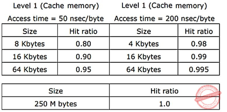
A computer system has a three level memory hierarchy, with access time and hit ratios as shown below:
(a) What should be the minimum sizes of level 1 and 2 memories to achieve an average access time of less than 100 nsec?
(b) What is the average access time achieved using the chosen sizes of level 1 and level 2 memories?
Theory Explanation. |
Question 28 |
RST 7.5 interrupt in 8085 microprocessor executes the interrupt service routine from interrupt vector location
0000H | |
0075H | |
003CH | |
0034H |
→ 60 in hexa decimal is 003CH.
Question 29 |
Purpose of a start bit in RS 232 serial communication protocol is
to synchronize receiver for receiving every byte | |
to synchronize receiver for receiving a sequence of bytes | |
a parity bit | |
to synchronize receiver for receiving the last byte |
Question 30 |
The correct matching for the following pairs is
(A) DMA I/O                    (1) High speed RAM
(B) Cache                      (2) Disk
(C) Interrupt I/O              (3) Printer
(D) Condition Code Register    (4) ALU
A – 4 B – 3 C – 1 D – 2 | |
A – 2 B – 1 C – 3 D – 4
| |
A – 4 B – 3 C – 2 D – 1 | |
A – 2 B – 3 C – 4 D – 1 |
Cache → High speed RAM
Interrupt I/O → Printer
Condition code register → ALU
Question 31 |
When an interrupt occurs, an operating system
ignores the interrupt | |
always changes state of interrupted process after processing the interrupt | |
always resumes execution of interrupted process after processing the interrupt
| |
may change state of interrupted process to 'blocked’ and schedule another process
|
Option B: Not always.
Option C: Not always. If some high priority interrupt comes during execution of current interrupt then it fails.
Option D: It is True always.
Question 32 |
The expression (a*b)* c op....
where 'op' is one of '+', '*' and '↑' (exponentiation) can be evaluated on a CPU with a single register without storing the value of (a * b) if
‘op’ is ’+’ or ‘*’ | |
‘op’ is ’↑’ or ‘*’ | |
‘op’ is ’↑’ or ‘+’ | |
not possible to evaluate without storing |
(a*b)*c + d
(a*b)*c * d
(a*b)*c ∧ d
In any case, brackets has the highest priority always. So I have to compute brackets first. Now, for + and *, I can do the rest of the operation and save results in the same register. But for exponentiation, I have to store the result of a*b, then do the computation of c∧d, then multiply these two results.
Hence, (A) is correct.
Question 33 |
Contents of A register after the execution of the following 8085 microprocessor program is
MVI  A, 55 H
MVI  C, 25 H
ADD  C
DAA
7AH | |
80H | |
50H | |
22H |
Question 34 |
A micro instruction into be designed to specify
- (a) none or one of the three micro operations of one kind and
(b) none or upto six micro operations of another kind
The minimum number of bits in the micro-instruction is
9 | |
5 | |
8 | |
None of the above |
So, no. of bits required
⌈log2 (3)⌉ = 2
(b) This is a horizontal micro-programming because at any given time atmost six micro-operations will be activated.
So, no. of bits required = 6
So, total minimum no. of bits required = 6+2 = 8
Question 35 |
A 32-bit wide main memory unit with a capacity of 1 GB is built using 256M × 4-bit DRAM chips. The number of rows of memory cells in the DRAM chip is 214. The time taken to perform one refresh operation is 50 nanoseconds. The refresh period is 2 milliseconds. The percentage (rounded to the closest integer) of the time available for performing the memory read/write operations in the main memory unit is _________.
59% | |
60% | |
61% | |
62% |
There are 214 rows, so time taken to refresh all the rows = 214 * 50ns = 0.82 milliseconds
It is given that total refresh period is 2ms. The refresh period contains the time to refresh all the rows and also the time to perform read/write operation.
So % time spent in refresh = (Time taken to refresh all rows / refresh period)*100
= (0.82 ms / 2ms)*100
= 41%
So the % of time for read/write operation = 100 - 41 = 59%
Question 36 |
(P) The processor pushes the process status of L onto the control stack.
(Q) The processor finishes the execution of the current instruction.
(R) The processor executes the interrupt service routine.
(S) The processor pops the process status of L from the control stack.
(T) The processor loads the new PC value based on the interrupt.
QPTRS | |
PTRSQ | |
TRPQS | |
QTPRS |
(Q) The processor finishes the execution of the current instruction
(P) The processor pushes the process status of L onto the control stack
(T) The processor loads the new PC value based on the interrupt
(R) The processor executes the interrupt service routine
(S) The processor pops the process status of L from the control stack
This is the sequence because when a process is in the middle of execution if an interrupt comes then that process execution is completed then the interrupt is serviced.
Question 37 |
I. Register-to-register arithmetic operations only
II. Fixed-length instruction format
III. Hardwired control unit
Which of the characteristics above are used in the design of a RISC processor?
I and II only | |
II and III only | |
I and III only | |
I, II and III |
So option D is the correct answer.
Question 38 |
The size of the physical address space of a processor is 2P bytes. The word length is 2W bytes. The capacity of cache memory is 2N bytes. The size of each cache block is 2M words. For a K-way set-associative cache memory, the length (in number of bits) of the tag field is
P - N - log2K | |
P - N + log2K | |
P - N - M - W - log2K | |
P - N - M - W + log2K |
Each word is of size 2W bytes.
Number of words in physical memory = 2(P-W)
So the physical address is P-W bits
Cache size is 2N bytes.
Number of words in the cache = 2(N-W)
Block size is 2M words
No. of blocks in the cache = 2(N-W-M)
Since it is k-way set associative cache, each set in the cache will have k blocks.
No. of sets = 2(N-W-M ) / k
SET bits = N-W-M-logk
Block offset = M
TAG bits = P-W-(N-M-W-logk)-M = P-W-N+M+W+logk-M = P - N + logk
Question 39 |
Type-1, Type-2, Type-3 and Type-4. Type-1 category consists of four instructions, each with 3 integer register operands (3Rs).
Type-2 category consists of eight instructions, each with 2 floating point register operands (2Fs).
Type-3 category consists of fourteen instructions, each with one integer register operand and one floating point register operand (1R+1F).
Type-4 category consists of N instructions, each with a floating point register operand (1F).
The maximum value of N is ________.
32 | |
33 | |
34 | |
35 |
So, total number of instruction encodings = 216
There are 16 possible integer registers, so no. of bits required for an integer operand = 4
There are 64 possible floating point registers, so no. of bits required for a floating point operand = 6
Type-1 instructions:
There are 4 type-1 instructions and each takes 3 integer operands.
No. of encodings consumed by type-1 = 4 × 24 × 24 × 24 = 214.
Type-2 instructions:
There are 8 type-2 instructions and each takes 2 floating point operands.
No. of encodings consumed by Type-2 instructions = 8 × 26 x 26 = 215.
Type-3 instructions:
There are 14 type-3 instructions and each takes one integer operand and one floating point operand.
No. of encodings consumed by Type-3 instructions = 14 × 24 × 26 = 14336.
So, no. of encodings left for Type-4 = 216 − (214 + 215 + 14336) = 2048.
Since type-4 instructions take one floating point register, no. of different instructions of Type-4 = 2048 / 64 = 32.
Question 40 |
The instruction pipeline of a RISC processor has the following stages: Instruction Fetch (IF), Instruction Decode (ID), Operand Fetch (OF), Perform Operation (PO) and Writeback (WB). The IF, ID, OF and WB stages take 1 clock cycle each for every instruction. Consider a sequence of 100 instructions. In the PO stage, 40 instructions take 3 clock cycles each, 35 instructions take 2 clock cycles each, and the remaining 25 instructions take 1 clock cycle each. Assume that there are no data hazards and no control hazards.
The number of clock cycles required for completion of execution of the sequence of instructions is ___________.
219 | |
220 | |
221 | |
222 |
Number of stages = 5
We know in a normal pipeline with k-stages time taken for n-instructions = k + n - 1 clock cycles.
So, in normal case total cycles = 100 + 5 - 1 = 104 cycles
But in this question it is given that PO stage of 40 instructions takes 3 cycles, 35 instructions takes 2 cycles and 25 instructions takes 1 cycle.
It is also given that all other stages take one clock cycle in all the 100 instructions.
PO stage of 40 instructions takes 3 cycles so these instructions will cause 2 stall cycle each, PO stage of 35 instructions takes 2 cycles so these instructions will cause 1 stall cycle each, But the 25 instruction whose PO stage takes 1 cycle, there are no stall cycles for these.
So, extra stall cycles = 40*2 + 35*1 = 80+35 = 115 cycles. So, total clock cycles = 104 + 115 = 219
Question 41 |
In serial communication employing 8 data bits, a parity bit and 2 stop bits, the minimum band rate required to sustain a transfer rate of 300 characters per second is
2400 band | |
19200 band | |
4800 band | |
1200 band |
(8+2+1+1) * 300
= 3600
Minimum band rate required is 4800 band.
Question 42 |
Which of the following devices should get higher priority in assigning interrupts?
Hard disk | |
Printer | |
Keyboard | |
Floppy disk |
Question 43 |
Which of the following addressing modes permits relocation without any change whatsoever in the code?
Indirect addressing | |
Indexed addressing | |
Base register addressing | |
PC relative addressing |
Question 44 |
Which of the following is true?
Unless enabled, a CPU will not be able to process interrupts. | |
Loop instructions cannot be interrupted till they complete. | |
A processor checks for interrupts before executing a new instruction. | |
Only level triggered interrupts are possible on microprocessors. |
Option 'C' also false. A processor checks for the interrupt before fetching an instruction.
Question 45 |
Formatting for a floppy disk refers to
arranging the data on the disk in contiguous fashion | |
writing the directory | |
erasing the system area | |
writing identification information on all tracks and sectors |
Question 46 |
The address space of 8086 CPU is
one Megabyte | |
256 Kilobytes | |
1 K Megabytes | |
64 Kilobytes |
Question 47 |
(a) Draw the schematic of an 8085 based system that can be used to measure the width of a pulse. Assume that the pulse is given as a TTL compatible signal by the source which generates it.
(b) Write the 8085 Assembly Language program to measure the width of the pulse. State all your assumption clearly.
Theory Explanation. |
Question 48 |
Calculate the total time required to read 35 sectors on a 2-sided floppy disk. Assume that each track has 8 sectors and the track-to-track step time is 8 milliseconds. The first sector to be read is sector 3 on track 10. Assume that the diskette is soft stored and the controller has a 1-sector buffer. The diskette spins at 300 RPM and initially, the head is on track 10.
Theory Explanation. |
Question 49 |
For a set-associative Cache Organization, the parameters are as follows:
- tc -- Cache access tine
tm -- Main memory access time
l -- number of sets
b -- block size
k*b -- set size
Calculate the hit ratio for a loop executed 100 times where the size of the loop is n * b and n= k * m is a non-zero integer and 1 < m ≤ l.
Given the value of the hit ratio for l = 1.
Theory Explanation. |
Question 50 |
The main memory of a computer has 2 cm blocks while the cache has 2c blocks. If the cache uses the set associative mapping scheme with 2 blocks per set, then block k of the main memory maps to the set
(k mod m) of the cache | |
(k mod c) of the cache | |
(k mod 2c) of the cache | |
(k mod 2 cm) of the cache |
= 2c/c
= c
∴ Cache set no. to which block k of main memory maps to
= (Main memory block no.) mod (Total set in cache)
= k mod c